Organic semiconductor structure, manufacturing method of the same, and organic semiconductor device
Inactive Publication Date: 2006-06-01
DAI NIPPON PRINTING CO LTD
View PDF3 Cites 19 Cited by
Summary
Abstract
Description
Claims
Application Information
AI Technical Summary
This helps you quickly interpret patents by identifying the three key elements:
Problems solved by technology
Method used
Benefits of technology
[0023] According to the manufacturing method of an organic semiconductor structure of the present invention, it is easy to form the organic semiconductor layer having few structural defects over a large area. Therefore, it is easy to obtain the organic semiconductor structure comprising the organic semiconductor layer having uniformalized charge transpor
Problems solved by technology
However, the organic semiconductor layers formed by the above-mentioned vacuum deposition process generally have characteristics that a large number of grain boundaries easily occur in polycrystalline state of aggregated fine crystals, and further, defects easily occur so that such grain boundaries and defects inhib
Method used
Image
Click on the blue label to locate the original text in one second.
Reading with bidirectional positioning of images and text.
Examples
example 1
(Preparation of Organic Semiconductor Device)
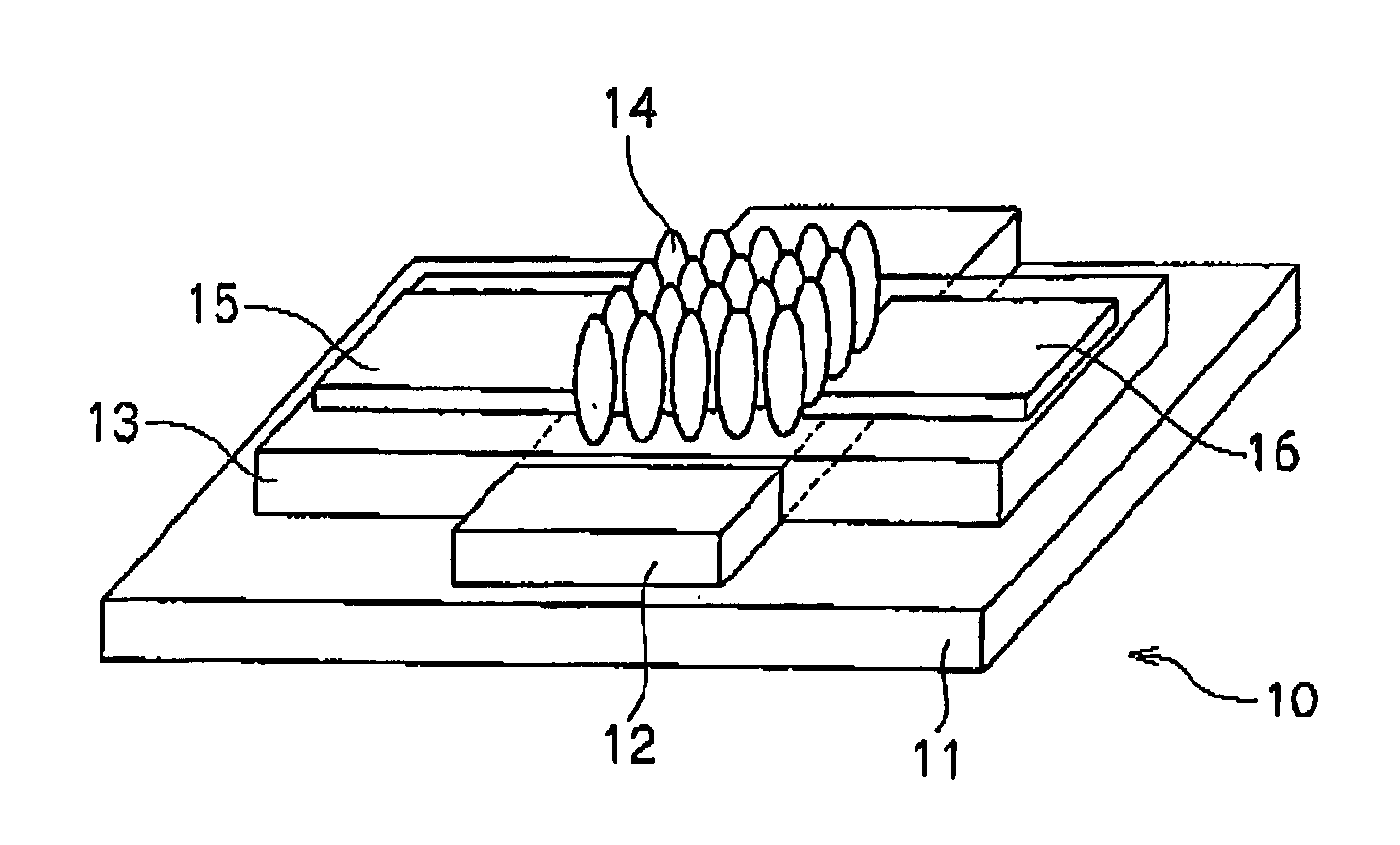
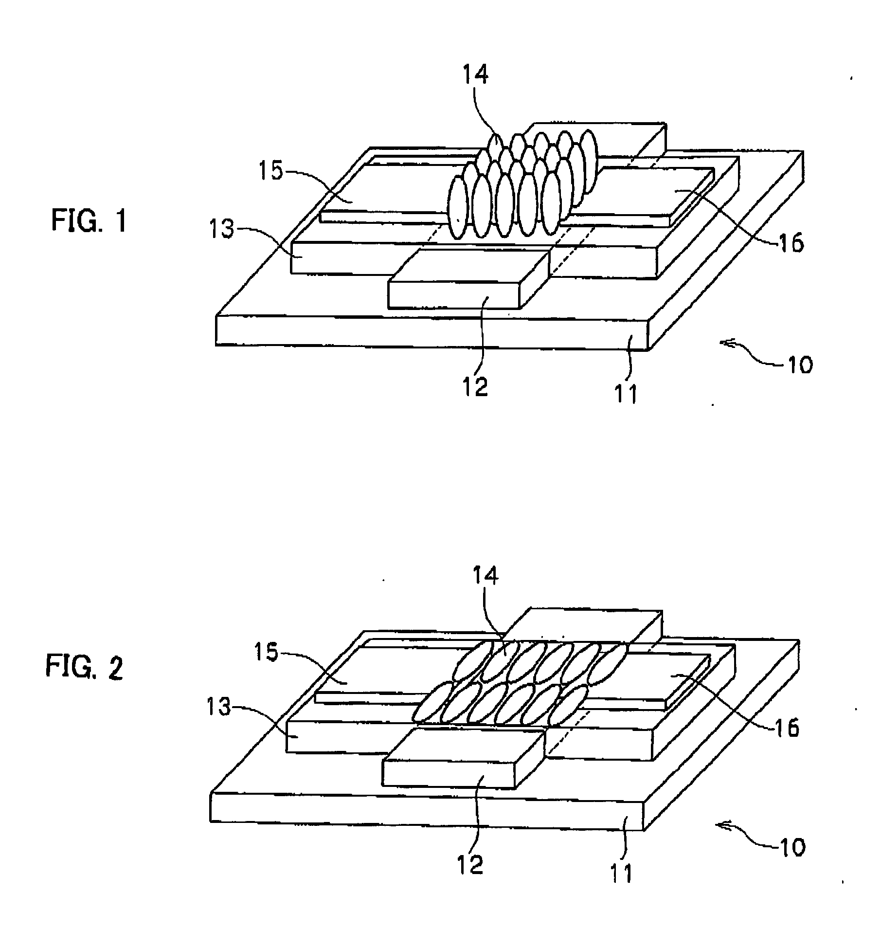
[0098] By using a phenyl naphthalene derivative (2-(4′-pentylphenyl)-6-methoxynaphthalene. Hereinafter, this may be abbreviated as 5-PNP-O1.), which is the compound shown in the above chemical formula 47, as the organic semiconductor material, the organic semiconductor device comprising substrate / gate electrode / gate-insulating layer (also serving as an liquid crystal alignment layer) / source-drain electrodes / organic semiconductor layer ( / protective layer) was prepared.
A glass substrate (thickness: 1.1 mm, Corning 1737) subjected to ultrasonic cleanings by using a neutral detergent, pure water, acetone and IPA in this order was used.
[0099] The gate electrode was formed on the substrate by resistance heating depositing a strap-shaped pattern (electrode width, 100 μm, between electrodes: 5 mm) of Au (thickness: 300 nm) via a metal mask, A similar electrode pattern can be formed by patterning an ITO electrode by using a wet process.
[0100...
example 2
[0106] As the liquid crystalline organic semiconductor material, 2-(4′-octylphenyl)-6-butyloxynaphthalene (abbreviated as 8-PNP-O4) shown in the above chemical formula 40 was used. Then, a sandwich cell, which was prepared by sticking two substrates provided with patterned ITO electrodes (electrode size: 4 mm×4 mm) together with 9 μm of cell gap, was heated to 150° C. In this sandwich cell, the liquid crystalline organic semiconductor material 8-PNP-O4 in the isotropic phase state was injected by the capillary phenomenon. Then, the liquid crystalline organic semiconductor material was supercooled, from the isotropic state, to around 115° C. at a speed of 1° C. / min. When grain formation of the smectic liquid crystal phase has begun partially, the temperature was raised to 140° C. at a speed of 20° C. / min, and by maintaining this temperature until the material is in the smectic liquid crystal state, the organic semiconductor layer of Example 2 was formed. In this organic semiconductor...
example 3
[0107] As the liquid crystalline organic semiconductor material, 2-(4′-octyloxyphenyl)-6-butyloxybenzothiazole (abbreviated as 80-PBT-O4) shown in the above chemical formula 48 was used. Then, a sandwich cell was prepared by sticking two substrates, provided with patterned ITO electrodes, together with 9 μm of cell gap. After that, this sandwich cell was heated to 150° C. In this cell, the liquid crystalline organic semiconductor material 80-PBT-O4 in the isotropic phase state was injected by the capillary phenomenon. Then, the liquid crystalline organic semiconductor material was supercooled, from the isotropic state, to around 100° C. at a speed of 1° C. / min. When grain formation of the smectic liquid crystal phase has begun partially, the temperature was raised to 103° C. at a speed of 20° C. / min, and by maintaining this temperature, the organic semiconductor layer of Example 3 was formed. This material turned into the nematic liquid crystal state during the supercooling process,...
PUM
Abstract
A manufacturing method of an organic semiconductor device wherein an organic semiconductor layer being, a structural component of an organic semiconductor device is formed continuously with uniform performance over a sufficiently large area. The organic semiconductor structure comprises an organic semiconductor layer formed from an organic semiconductor material having a liquid crystal molecule in at least one part, the liquid crystalline organic semiconductor material exhibits a supercooled state during a phase transition process, the phase of the material is transferred from the supercooled state to the phase having periodic regularity at a location of a center of gravity in between the liquid crystal molecules; in a temperature raising process from the phase having no periodic regularity a center of gravity in between the liquid crystal molecules, the liquid crystalline organic semiconductor material exhibiting the phase having no periodic regularity with of a center of gravity in between the liquid crystal molecules is supercooled, to a temperature lower than a temperature of which the phase is transferred to the phase having periodic regularity at a location with a center of gravity in between the liquid crystal molecules, and after the phase transition to the phase having periodic regularity at a location of a center of gravity in between the liquid crystal molecules is started, the material is turned into a state that the converted to a phase having periodic regularity at a location of with a center of gravity between the liquid crystal molecules being thermodynamically stable phase and the phase having no periodic regularity at a location of a center of gravity in between the liquid crystal molecules is a thermodynamically metastable phase, and the organic semiconductor layer being formed by maintaining said state until the liquid crystalline organic semiconductor material is turned into a converted to a state exhibiting the phase having periodic regularity at a location of a center of gravity in between the liquid crystal molecules.
Description
BACKGROUND OF THE INVENTION [0001] 1. Field of the Invention [0002] The present invention relates to an organic semiconductor structure comprising an organic semiconductor layer formed with organic semiconductor material having liquid crystallinity, a manufacturing method of the same and an organic semiconductor device. [0003] 2. Description of the Related Art [0004] As a typical example of an organic semiconductor device, an organic field-effect transistor (also called organic FET) using an organic semiconductor as an active layer (hereinafter, referred to as an organic semiconductor layer) can be mentioned. In order to realize a thin film-large area device, the organic FET is required to have uniform charge transport property over a sufficient large area. [0005] In this organic FET, the organic semiconductor layer is formed, by vacuum deposition process, from molecular crystals represented by pentacene (see Y.-Y. Lin, D. J. Gundlach, S. Nelson, and T. N. Jackson, “Stacked Pentacen...
Claims
Application Information
Patent Timeline
Application Date:The date an application was filed.
Publication Date:The date a patent or application was officially published.
First Publication Date:The earliest publication date of a patent with the same application number.
Issue Date:Publication date of the patent grant document.
PCT Entry Date:The Entry date of PCT National Phase.
Estimated Expiry Date:The statutory expiry date of a patent right according to the Patent Law, and it is the longest term of protection that the patent right can achieve without the termination of the patent right due to other reasons(Term extension factor has been taken into account ).
Invalid Date:Actual expiry date is based on effective date or publication date of legal transaction data of invalid patent.