Multilayer capacitor

a multi-layer capacitor and capacitor technology, applied in the direction of capacitors, fixed capacitor details, fixed capacitors, etc., can solve the problems of high cost of electrode materials, and easy generation of noise that includes many harmonic components, and achieves high design flexibility. the effect of low cost of electrode materials

Active Publication Date: 2008-09-02
MURATA MFG CO LTD
View PDF19 Cites 9 Cited by
  • Summary
  • Abstract
  • Description
  • Claims
  • Application Information

AI Technical Summary

Benefits of technology

[0022]In order to overcome the problems described above, preferred embodiments of the present invention provide a multi-terminal multilayer capacitor that has high design flexibility, low cost of electrode material, and hardly ever experiences any structural defect hardly.
[0035]Therefore, the length of opposed edges of the first and third internal electrodes, and the length of opposed edges of the second and fourth internal electrodes can be freely adjusted regardless of a pitch between the external terminal electrodes. Accordingly, lengthening or shortening of current paths can be relatively freely performed. For example, an ESR of a multilayer capacitor can be arbitrarily adjusted.
[0036]When adding a capacitor portion, for example, a third capacitor portion other than first and second capacitor portions, a capacitor portion can be added individually along the length of the first and second side surfaces. Thus, design flexibility of the multilayer capacitor can be enhanced.
[0037]In addition, according to various preferred embodiments of the present invention, capacitor-forming portions of the first and fourth internal electrodes do not overlap with one another, and capacitor-forming portions of the second and third internal electrodes do not overlap with each other. Therefore, in each internal electrode, a portion that is unnecessary from a capacitor-formation viewpoint is prevented from existing. Thus, ineffective use of an electrode material is prevented, and, in addition, a bonding area of adjacent dielectric layers for positioning each internal electrode at an interface between the layers is ensured, so that, in a laminate, a structural defect, such as delamination, can hardly occur.
[0038]According to preferred embodiments of the present invention, each internal electrode includes at least two lead portions. Regarding the positions of the lead portions, the lead portion of the first internal electrode and the lead portion of the second internal electrode are disposed so as to be alternately exposed along the length of each of the first and second side surfaces, and the lead portion of the third internal electrode and the lead portion of the fourth internal electrode are disposed so as to be alternately exposed along the length of each of the first and second side surfaces. Thus, a current flow in each internal electrode can be directed in various directions, and current flows in adjacent lead portions can be made opposite, so that magnetic fields can mutually cancel. As a result, an ESL can be reduced.
[0039]In a multilayer capacitor according to preferred embodiments of the present invention, the lead portion of the first internal electrode and the lead portion of the third internal electrode are disposed so as to be adjacent, and the lead portion of the second internal electrode and the lead portion of the fourth internal electrode are disposed so as to be adjacent, whereby an effect of magnetic field cancellation can be enhanced.

Problems solved by technology

When impedances of a power line and the ground in a power supply circuit cause large fluctuations in the power line, the operation of a driven circuit becomes unstable, interference between circuits via the power supply circuit occurs, and oscillation occurs.
Accordingly, noise that includes many harmonic components is easily generated, and, in an IC power supply circuit, stronger decoupling needs to be performed.
When counter electromotive force dV is large, supply of electric charge to the IC is delayed.
In circuit design, there is a limitation in reducing the inductances of the patterns.
Therefore, a method of adjusting the length of a current path by adjusting the lengths of the facing edges cannot be simply employed, and adjustment of an equivalent series resistance (ESR) of the multilayer capacitor 8 is not always facilitated.
As a result, the ESR tends to be low.
When the ESR is too low, there are problems in that inductance of a peripheral circuit causes a resonance phenomenon, so that power supply voltage greatly drops, or so that damped oscillation, such as ringing, easily occurs.
However, in the structure described in Japanese Unexamined Patent Application Publication No. 2002-151349, as described above, ESR adjustment is not always facilitated.
Accordingly, design flexibility is low, and, in addition, there is a problem in that, when adding capacitor portions, the laminate 6 is too elongated to cause a flexural strength of the laminate 6 to be low.
In addition, since a bonding area of adjacent dielectric layers 1 for positioning each of the common internal electrodes 21 and 22 at an interface is small, there is also a problem in that a structural defect, such as delamination, easily occurs in the laminate 6.
Thus, it is necessary to form the external terminal electrodes 13 on each of four side surfaces 2 to 5, so that there is a problem in that design flexibility is low.
Accordingly, from a capacitor formation viewpoint, there is a problem in that an electrode material is not effectively used.
In addition, similarly to the case of the Japanese Unexamined Patent Application Publication No. 2004-103883, in the structure described in Japanese Unexamined Patent Application Publication No. 2006-32904, a bonding area of adjacent dielectric layers 1 for positioning each of the internal electrodes 25 to 28 or 25a to 28a at an interface is small, so that there is a problem in that a structural defect, such as delamination, easily occurs in the laminate 6.

Method used


Image

  • Multilayer capacitor
  • Multilayer capacitor
  • Multilayer capacitor

Examples


Embodiment Construction

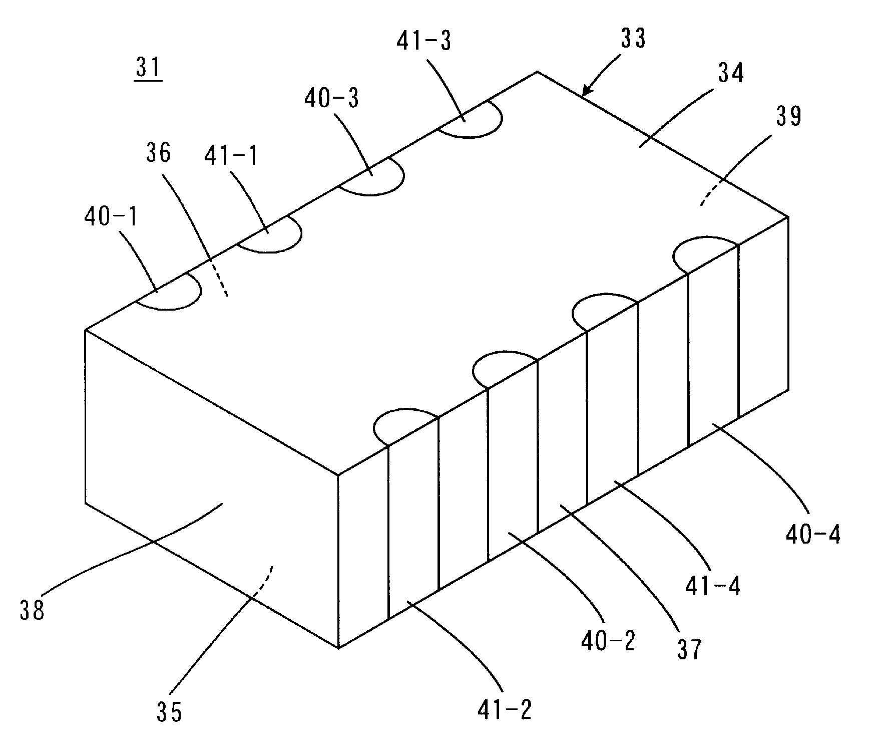
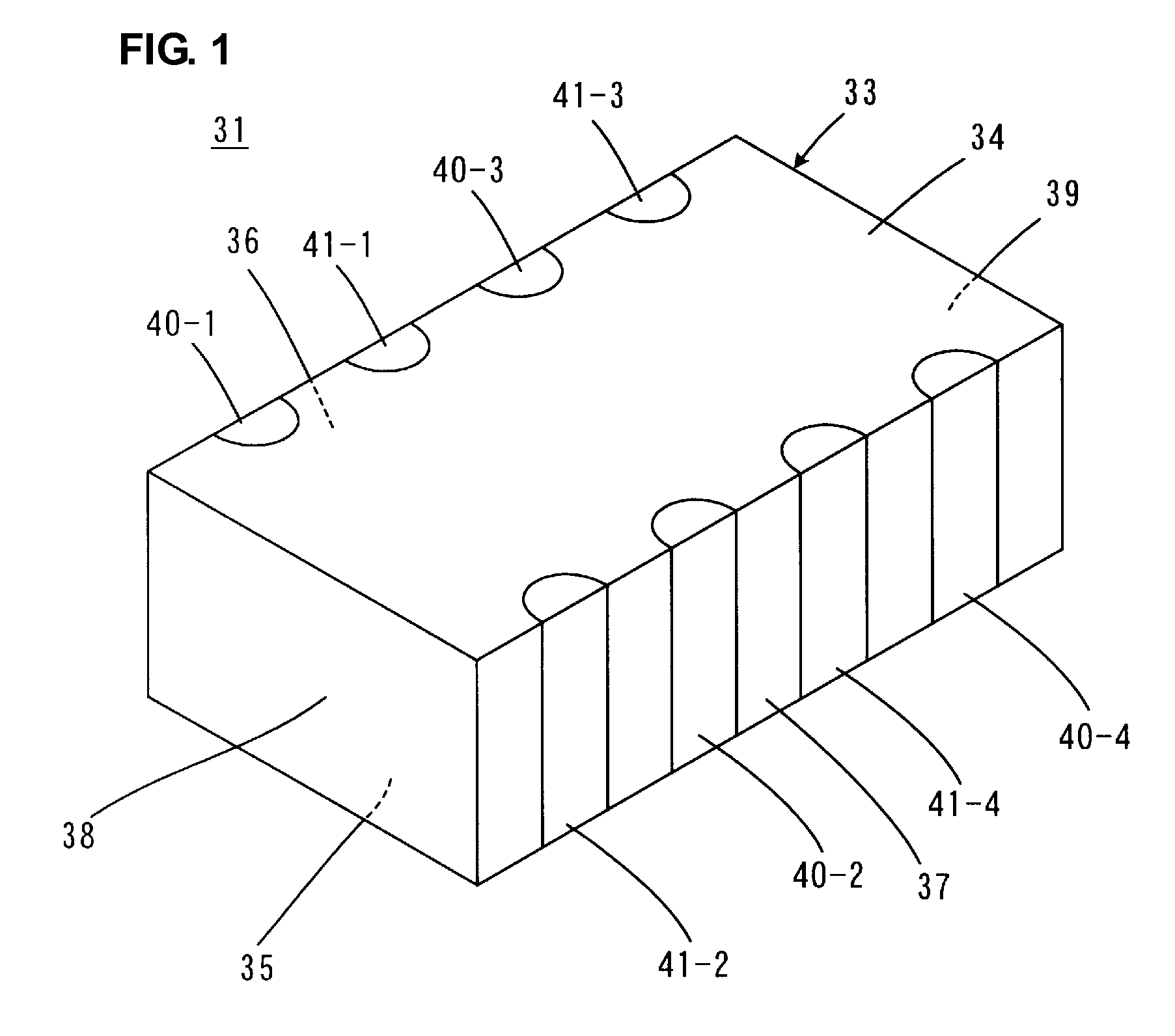
[0062]FIGS. 1 to 4 illustrate a multilayer capacitor 31 according to a first preferred embodiment of the present invention. FIG. 1 is a perspective view showing the exterior of the multilayer capacitor 31. FIG. 2 is a plan view showing the exterior of the multilayer capacitor 31. FIGS. 3A and 3B are plan views showing an internal structure of the multilayer capacitor 31 by using particular sections. FIGS. 4A and 4B are the same plan views as FIGS. 3A and 3B, including dashed line arrows indicating the flows of currents.

[0063]The multilayer capacitor 31 includes a laminate 33 that preferably has a substantially rectangular parallelepiped shape and is preferably formed by laminating a plurality of dielectric layers 32. Each dielectric layer 32 is preferably formed of dielectric ceramic consisting primarily of, for example, BaTiO3, CaTiO3, SrTiO3, CaZrO3, or the like. An accessory component, such as a Mn compound, a Fe compound, a Cr compound, a Co compound, or a Ni compound, may be ad...


PUM


Abstract

A multi-terminal multilayer capacitor reducing an equivalent series inductance (ESL), whose design flexibility is high, in which cost of electrode material is low, and in which a structural defect hardly occurs includes lead portions of first and second internal electrodes and lead portions of third and fourth internal electrodes that are disposed along the length of each of two side surfaces so as to be alternately exposed. Preferably, the first and third internal electrodes, and the second and fourth internal electrodes are disposed so as to be arranged along the length of each side surface in a coplanar manner, with a predetermined distance provided between two internal electrodes. When viewed in a laminating direction of dielectric layers, a capacitor-forming portion of the first internal electrode does not overlap with a capacitor-forming portion of the fourth internal electrode, and a capacitor-forming portion of the second internal electrode does not overlap with a capacitor-forming portion of the third internal electrode.

Description

BACKGROUND OF THE INVENTION[0001]1. Field of the Invention[0002]The present invention relates to multilayer capacitors, and in particular, to a multilayer capacitor that is a multi-terminal type that reduces an equivalent series inductance (ESL).[0003]2. Description of the Related Art[0004]When impedances of a power line and the ground in a power supply circuit cause large fluctuations in the power line, the operation of a driven circuit becomes unstable, interference between circuits via the power supply circuit occurs, and oscillation occurs. Accordingly, a decoupling capacitor is normally connected between the power line and the ground. The decoupling capacitor has a role of suppressing fluctuation in power-supply voltage and interference between circuits by reducing the impedance between the power line and the ground.[0005]In recent years, in communication devices such as cellular phones and information processing devices such as personal computers, signal speed has been increas...

Claims


Application Information

Patent Timeline
Patent Type & Authority Patents(United States)
IPC IPC(8): H01G4/06
CPCH01G4/012H01G4/30H01G4/232
Inventor OTA, TETSUHIKO
Owner MURATA MFG CO LTD
Why Eureka
Try Eureka