Method for manufacturing semiconductor substrate

a manufacturing method and semiconductor technology, applied in the direction of semiconductor devices, electrical equipment, basic electric elements, etc., can solve the problems of bonded substrates or soi substrates broken or cracked

Active Publication Date: 2009-04-30
SHIN ETSU CHEM IND CO LTD
View PDF2 Cites 7 Cited by
  • Summary
  • Abstract
  • Description
  • Claims
  • Application Information

AI Technical Summary

Benefits of technology

[0014]In the present invention, since the gate oxide film formed on the SOI substrate is obtained by laminating the low-temperature thermal oxide film grown at a temperature of 450° C. or below and the oxide film formed based on the CVD method, the underlying thermal oxide film can suppress a structural defect, e.g., an interface state, and the CVD oxide film formed on the thermal oxide film enables adjusting a thickness of the gate oxide film. According to such a technique, a conventional general silicon oxide film forming apparatus can be used to form the gate oxide film at a low temperature, thereby achieving a consistent reduction in temperature in the SOI substrate manufacturing process.

Problems solved by technology

However, since each of these transparent insulator substrate has a thermal expansion coefficient greatly different from that of a silicon crystal, there occurs a problem that a bonded substrate or an SOI substrate is broken or cracked when a manufacturing process of the SOI substrate includes a high-temperature process.

Method used


Image

  • Method for manufacturing semiconductor substrate
  • Method for manufacturing semiconductor substrate

Examples


example

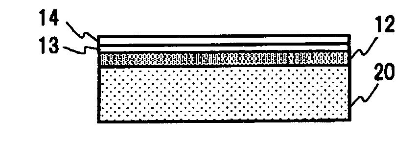
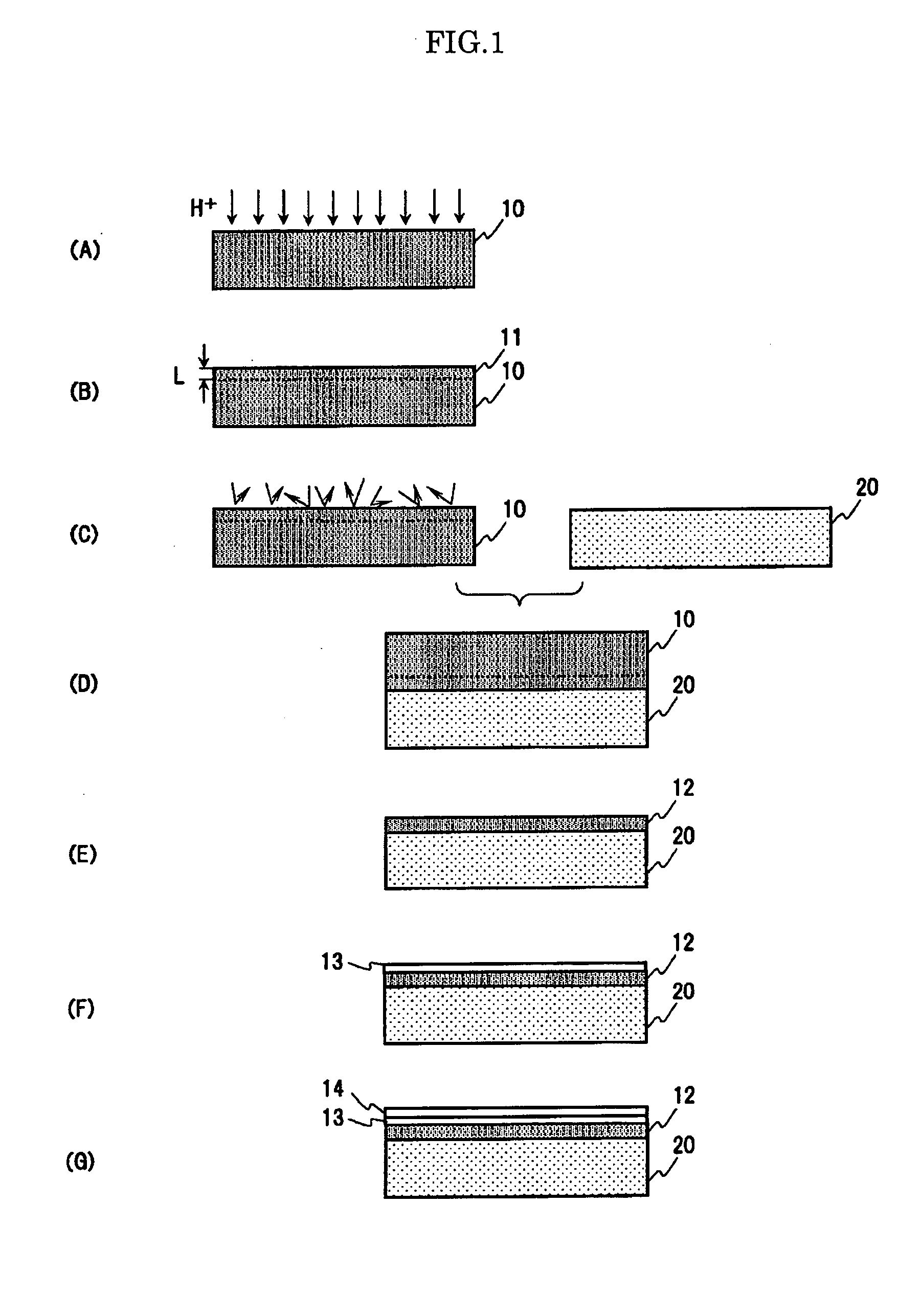
[0017]FIG. 1 is a view for explaining a process example of a method for manufacturing a semiconductor substrate according to the present invention. A silicon substrate 10 depicted in FIG. 1(A) is generally a single-crystal Si substrate, and a support substrate is a quartz substrate 20. Here, the single-crystal Si substrate 10 is, for example, a generally commercially available Si substrate grown based on a CZ method (Czochralski method), and an electrical characteristic value such as a conductivity type and a specific resistance, a crystal orientation, or a crystal diameter thereof is appropriately selected in dependence on a design value or a process of a device adopting an SOI substrate manufactured by the method according to the present invention or a display area of a device to be manufactured. It is to be noted that an oxide film may be formed in advance on a surface (a bonding surface) of this single-crystal Si substrate 10 by a method such as thermal oxidation.

[0018]The singl...


PUM

PropertyMeasurementUnit
temperatureaaaaaaaaaa

Abstract

A consistent reduction in temperature in an SOI substrate manufacturing process is achieved.
A gate oxide film provided on an SOI substrate is obtained by laminating a low-temperature thermal oxide film 13 grown at a temperature of 450° C. or below and an oxide film 14 obtained based on a CVD method. Since the thermal oxide film 13 is a thin film of 100 Å or below, a low temperature of 450° C. or below can suffice. The underlying thermal oxide film 13 can suppress a structural defect, e.g., an interface state, and the CVD oxide film 14 formed on the thermal oxide film can be used to adjust a thickness of the gate oxide film. According to such a technique, a conventional general silicon oxide film forming apparatus can be used to form the gate oxide film at a low temperature, thereby achieving a consistent reduction in temperature in the SOI substrate manufacturing process.

Description

BACKGROUND OF THE INVENTION[0001]1. Field of the Invention[0002]The present invention relates to a method for manufacturing a semiconductor substrate having a silicon film on a transparent insulator substrate.[0003]2. Description of the Related Art[0004]As a semiconductor substrate that enables high performances of a semiconductor device, an SOI (Silicon On Insulator) substrate is attracting attention (see, e.g., Japanese Patent No. 3048201 or A. J. Auberton-Herve et al., “SMART CUT TECHNOLOGY: INDUSTRIAL STATUS of SOI WAFER PRODUCTION and NEW MATERIAL DEVELOPMENTS” (Electrochemical Society Proceedings Volume 99-3 (1999) p. 93-106).). That is because adopting an SOI structure to bury an oxide film below a single-crystal silicon thin film enables reducing a parasitic capacitance, improving an operating speed, and suppressing a power consumption.[0005]When the SOI substrate is utilized as an optical device, a support substrate that is bonded to a silicon substrate must be a transparen...

Claims


Application Information

Patent Timeline
Patent Type & Authority Applications(United States)
IPC IPC(8): H01L21/762
CPCH01L21/2007H01L21/26506H01L21/28167H01L29/78603H01L21/32105H01L21/76254H01L29/4908H01L21/3144H01L21/02216H01L21/02238H01L21/02255H01L21/02271H01L21/02211H01L21/20H01L21/205H01L21/18H01L21/02337
Inventor AKIYAMA, SHOJIKUBOTA, YOSHIHIROITO, ATSUOKAWAI, MAKOTOTOBISAKA, YUUJITANAKA, KOICHI
Owner SHIN ETSU CHEM IND CO LTD
Why Eureka
Try Eureka