
Direct growth of metal nanoplates on semiconductor substrates

a technology of metal nanoplates and substrates, applied in the direction of sustainable manufacturing/processing, semiconductor/solid-state device details, final product manufacturing, etc., can solve problems such as surface roughness, and achieve the effects of large facial area, large facial area, and high production efficiency

Inactive Publication Date: 2012-08-21
UCHICAGO ARGONNE LLC
View PDF25 Cites 4 Cited by
  • Summary
  • Abstract
  • Description
  • Claims
  • Application Information

AI Technical Summary

Benefits of technology

This method enables the fabrication of pristine metal / semiconductor composite materials with improved performance by creating clean interfaces and tunable nanostructures, enhancing stability and efficiency in applications like photovoltaic cells and catalysis.

Problems solved by technology

The existence of defects typically results from the surface roughness and crystalline defects of the semiconductor wafer substrate itself.

Method used


Image

  • Direct growth of metal nanoplates on semiconductor substrates
  • Direct growth of metal nanoplates on semiconductor substrates
  • Direct growth of metal nanoplates on semiconductor substrates

Examples


example 1

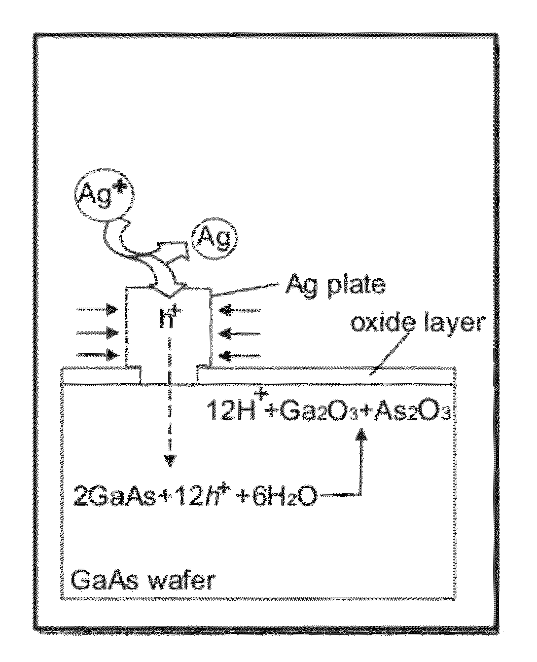
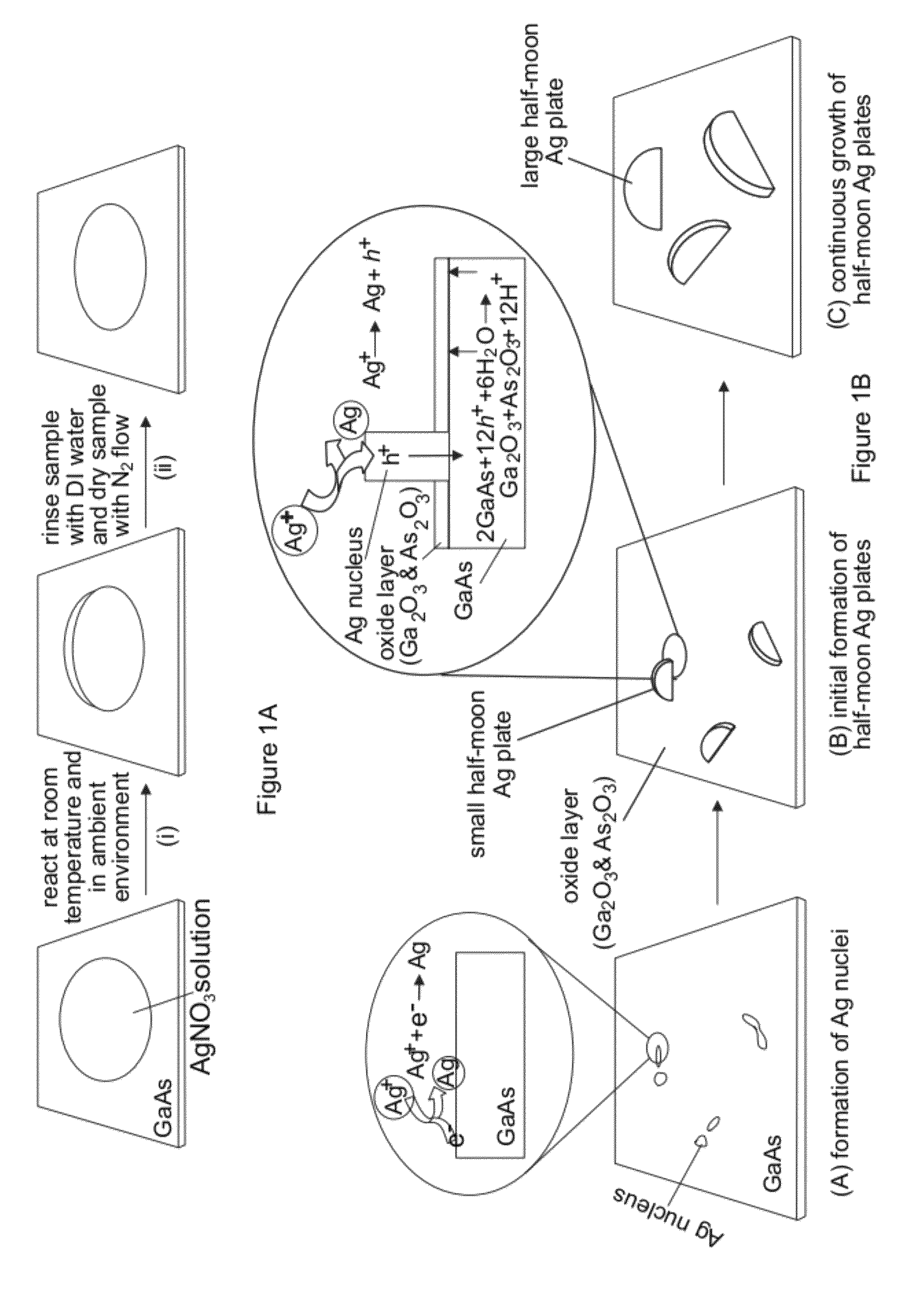
[0090]With reference to FIGS. 12A-12C, the nucleation and growth of Ag nanoplates on an n-type single crystal GaAs substrate through reaction with a substantially pure aqueous solution of AgNO3 is illustrated. In a typical synthesis, a droplet of aqueous solution of AgNO3 with appropriate concentration, from about 0.1 M to about 10 M, is delivered to the surface of a piece of n-type GaAs wafer that has been cleaned by soaking in a dilute 2% hydrofluoric acid (HF) solution for 5 minutes. Contacting the GaAs wafer with AgNO3 solution immediately leads to quick reduction of Ag+ by the surface electrons (as shown in FIG. 12A), resulting in the formation of small Ag clusters (i.e., nuclei) on the nucleation sites (usually surface defects) on the GaAs surface. Once the nuclei are formed, hole injection process dominates the growth of the nuclei into larger Ag particles because the equilibrium potential (greater than or equal to 0.74 V versus NHE for AgNO3 solutions with concentrations hig...

example 2

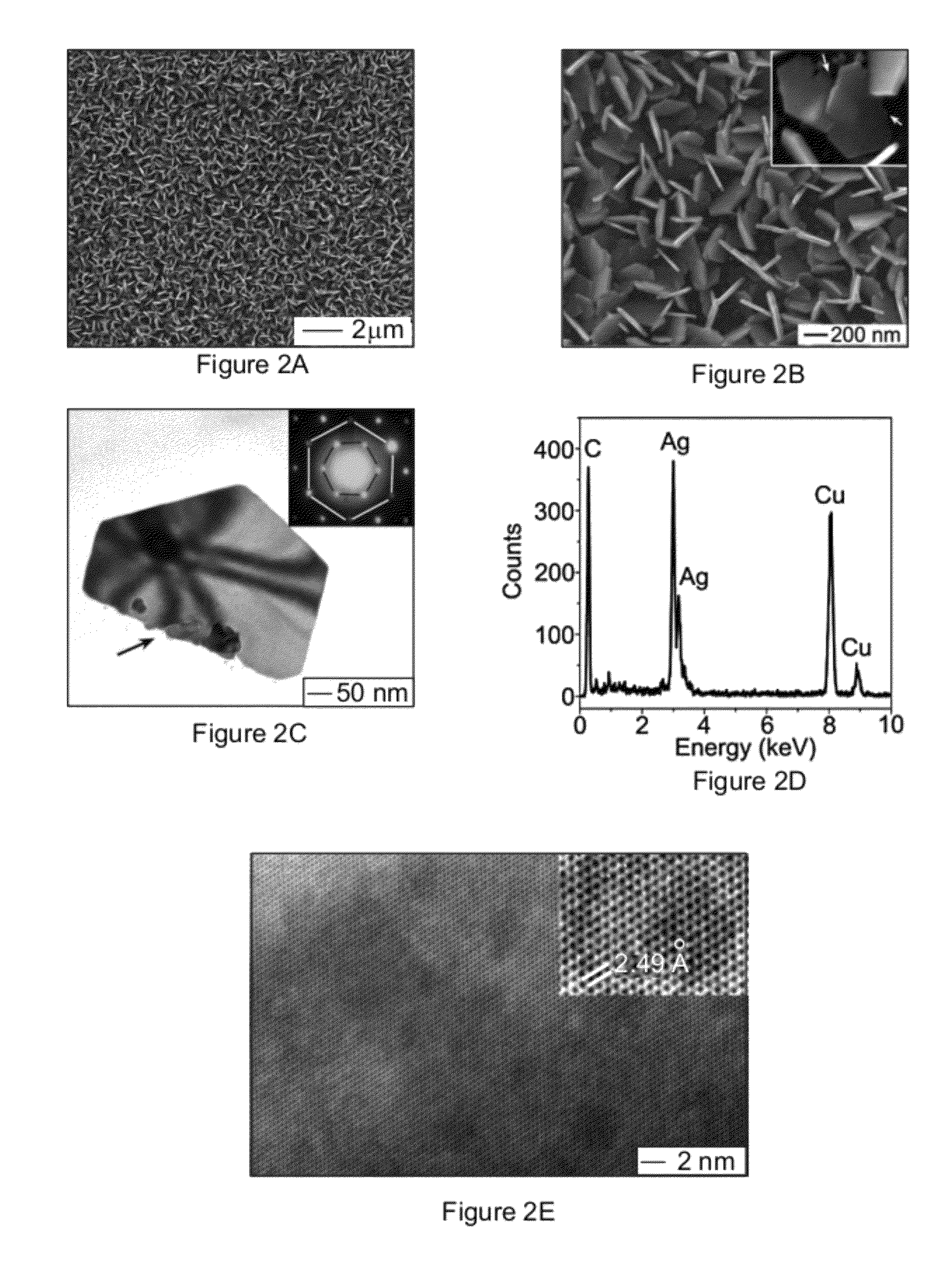
[0096]The size of the nanoplates can be tuned by controlling the growth time. FIGS. 14A and 14B compare the Ag nanoplates obtained by reacting n-GaAs wafers (with dopant concentration of 1×1018 cm−3) with a 2 M AgNO3 solution for 30 seconds and 60 seconds, respectively. The nanoplate sizes, which are determined by measuring the lengths of the orthographic projections of individual nanoplates along their longitudinal axes in the surface of the substrate, increase from about 125 nm to about 210 nm with increasing growth time from 30 seconds to 60 seconds. On the other hand, the thicknesses of the nanoplates remain substantially constant at about 22 nm. The dimensional evolution of the Ag nanoplates upon growth time indicates that growing a Ag nanoplate may start with the formation of a Ag nucleus at a defect site of the GaAs surface because the defect site has higher surface energy, thus higher reactivity, than adjacent flat areas. The lateral dimension of the Ag nucleus may be consis...

example 3

[0097]The thicknesses of Ag nanoplates can also be finely tuned by controlling the concentration of AgNO3 solution. Silver nanoplates with smooth surfaces can be achieved on the n-GaAs wafers by reacting with AgNO3 solutions with concentrations ranging from 1 M to saturation concentration, about 10 M. FIGS. 14D and 14E show typical SEM images of the samples prepared through reactions with 6 M and 8 M AgNO3 solutions for 60 seconds, respectively. The comparison between the samples grown with different concentrations of AgNO3 solutions for the same time, 60 seconds, indicates that the thicknesses of nanoplates increase with concentrations of the AgNO3 solutions but their sizes remain substantially constant. The independence of the sizes of the Ag nanoplates on the concentrations of AgNO3 solutions implies that the rate for adding Ag atoms to the peripheral edge surfaces of the nanoplates is determined by the kinetics of the hole injection process rather than the diffusion of Ag+ ions....


PUM

PropertyMeasurementUnit
thicknessaaaaaaaaaa
diameteraaaaaaaaaa
contact anglesaaaaaaaaaa

Abstract

Metal nanoplates are grown on n-type and p-type semiconductor wafer substrates through galvanic reactions between substantially pure aqueous metal solutions and the substrates. The morphology of the resulting metal nanoplates that protrude from the substrate can be tuned by controlling the concentration of the metal solution and the reaction time of the solution with the semiconductor wafer. Nanoplate size gradually increases with prolonged growth time and the nanoplate thicknesses increases in a unique stepwise fashion due to polymerization and fusion of adjacent nanoplates. Further, the roughness of the nanoplates can also be controlled. In a particular embodiment, Ag nanoplates are grown on a GaAs substrate through reaction with a solution of AgNO3 with the substrate.

Description

CROSS REFERENCE TO RELATED PATENT APPLICATIONS[0001]The present application claims priority to U.S. Provisional Patent Application No. 61 / 104,591, filed Oct. 10, 2008, incorporated herein by reference in its entirety.STATEMENT OF GOVERNMENT INTEREST[0002]The United States Government claims certain rights in this invention pursuant to Contract No. W-31-109-ENG-38 between the United States Government and the University of Chicago and / or pursuant to DE-AC02-06CH11357 between the United States Government and UChicago Argonne, LLC representing Argonne National Laboratory.FIELD OF THE INVENTION[0003]The present invention relates generally to the field of nanostructures formed on substrates. More particularly, the invention relates to methods for growing metal nanostructures, such as Ag, Ag / Au, Ag / Pt, and Ag / Pd from solutions of metal precursors on semiconductor substrates through galvanic reactions.BACKGROUND OF THE INVENTION[0004]This section is intended to provide a background or contex...

Claims


Application Information

Patent Timeline
Patent Type & Authority Patents(United States)
IPC IPC(8): H01L21/44
CPCC23C18/1642C23C18/1689C23C18/42C23C18/48C23C18/54H01L31/184B82Y30/00Y02E10/544Y02P70/50
Inventor SUN, YUGANG
Owner UCHICAGO ARGONNE LLC
Learn More