Display device and electronic device including the same

a technology of electronic devices and display devices, applied in semiconductor devices, instruments, electrical devices, etc., can solve the problems of insufficient characteristics of transistors formed using conventional oxide semiconductors, and achieve the effects of low power consumption, low field effect mobility, and low off curren

Active Publication Date: 2012-08-21
SEMICON ENERGY LAB CO LTD
View PDF128 Cites 71 Cited by
  • Summary
  • Abstract
  • Description
  • Claims
  • Application Information

AI Technical Summary

Benefits of technology

[0006]The field effect mobility of a transistor in which a channel region is formed in an oxide semiconductor is higher than that of a transistor in which a channel region is formed in amorphous silicon. The field effect mobility of a transistor formed using amorphous silicon is approximately 0.5 cm2 / Vs in general, whereas the field effect mobility of a transistor formed using an oxide semiconductor is 10 cm2 / Vs to 20 cm2 / Vs. In addition, an active layer can be formed using an oxide semiconductor by a sputtering method or the like, and a manufacturing process thereof is simpler than that of a transistor including polycrystalline silicon formed using a laser device.

Problems solved by technology

However, when not only a pixel but also a driver circuit is formed using a transistor formed using an oxide semiconductor, a transistor formed using a conventional oxide semiconductor does not have sufficient characteristics.

Method used


Image

  • Display device and electronic device including the same
  • Display device and electronic device including the same
  • Display device and electronic device including the same

Examples


embodiment 1

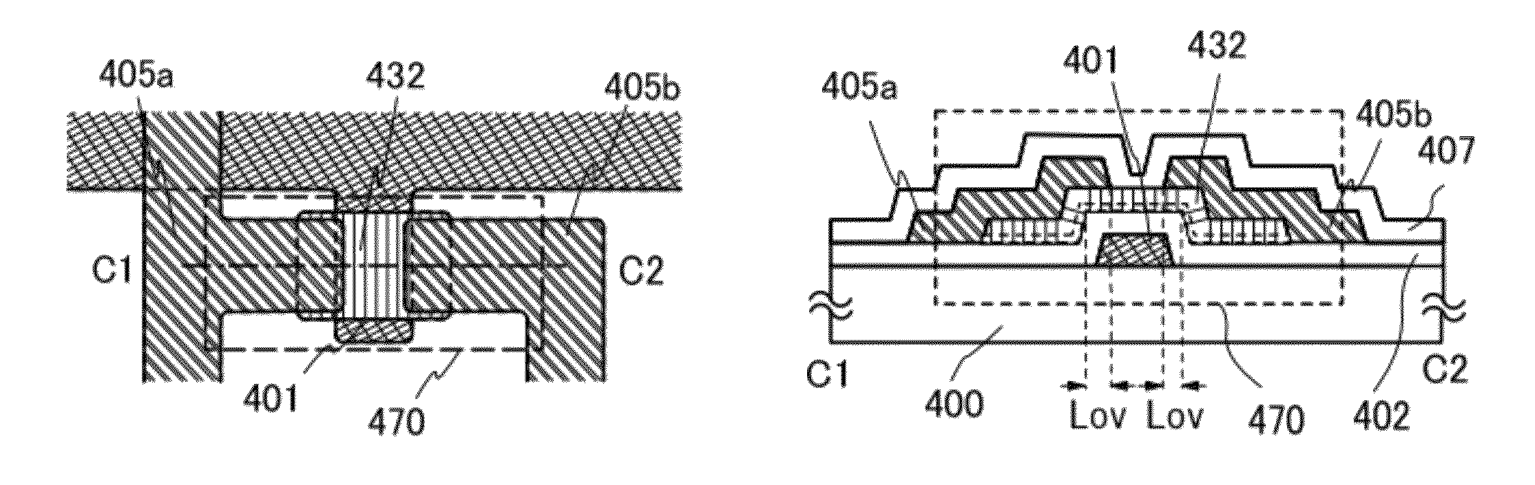
[0094]FIGS. 4A and 4B show an embodiment of the present invention. FIG. 4A illustrates a display device provided with a pixel portion 1502, gate drivers 1503 and 1504, and an analog switch 1505 for driving a source line integrated on a glass substrate 1501. The reason why the analog switch 1505 is used for driving the source line is as follows. For example, in the case of a full high-vision display device, there are 5760 (1920×RGB) source signal lines. When a source driver is not formed over the same substrate as the source signal lines, terminals of the source signal lines are each connected to a terminal of the source driver. Therefore, there is a problem in that a contact failure of a terminal easily occurs due to mechanical impact or the like. Reduction in the number of terminals is effective for less contact failure. Accordingly, an object is to reduce the number of terminals by forming an analog switch array over the same substrate as the source signal lines and selectively co...

embodiment 2

[0099]FIGS. 6A and 6B each illustrate an embodiment of a display device provided with a source driver. FIG. 6A illustrates an example in which a pixel portion 1702, gate drivers 1703 and 1704, and a source driver 1705 are provided over a glass substrate 1701. The gate drivers 1703 and 1704 and the source driver 1705 are supplied with signals from FPCs 1706 and 1707. A left side and a right side of the display device are provided with the gate driver 1703 and the gate driver 1704, respectively, and a pixel is driven; thus, driving can be performed with half of driving capability as compared to the case where a gate driver is provided on only one side.

[0100]FIG. 6B illustrates an example in which, over a glass substrate 1711, a pixel portion 1712, gate drivers 1713, 1714, 1715, and 1716 on an upper side and a lower side of a display device, and source drivers 1717, 1718, 1719, and 1720 on a left side and a right side of the display device are provided. The gate drivers and the source ...

embodiment 3

[0101]Calculation results in the case where an analog switch is used for driving a source line are show below. The calculation is made in the case of a 100-inch liquid crystal display device with a frame frequency of 240 Hz (quadruple frame rate). As described above, a source line needs to be written within 0.7 μs at a quadruple frame rate. At this time, a transistor used for the analog switch for sampling has L / W=3 μm / 1500 μm, a field effect mobility of 100 cm2 / Vs, and a threshold voltage of 1.5 V. A source signal line has a sheet resistance of 0.01 Ω / square, a resistance of 2.08 KΩ, a capacity of 18.5 pF, and a line width of 6 μm. An aim is to perform writing until a source line potential reaches 99.9% of an expected value.

[0102]FIG. 7 shows a relation between rise time of a gate line and a size of a display device. When the maximum delay time of the gate wiring is set to 0.5 μs, the delay time of the gate line can satisfy the requirement even with a 100-inch display device. In th...


PUM


Abstract

One embodiment of the present invention provides a highly reliably display device in which a high mobility is achieved in an oxide semiconductor. A first oxide component is formed over a base component. Crystal growth proceeds from a surface toward an inside of the first oxide component by a first heat treatment, so that a first oxide crystal component is formed in contact with at least part of the base component. A second oxide component is formed over the first oxide crystal component. Crystal growth is performed by a second heat treatment using the first oxide crystal component as a seed, so that a second oxide crystal component is formed. Thus, a stacked oxide material is formed. A transistor with a high mobility is formed using the stacked oxide material and a driver circuit is formed using the transistor.

Description

TECHNICAL FIELD[0001]The present invention relates to a display device including an oxide semiconductor, a manufacturing method thereof, and an electronic appliance including the display device.BACKGROUND ART[0002]Transistors formed over a glass substrate or the like are typically manufactured using amorphous silicon, polycrystalline silicon, or the like, as typically seen in liquid crystal display devices. Although transistors including amorphous silicon have low field effect mobility, they can be formed over a larger glass substrate. On the other hand, although transistors including polycrystalline silicon have high field effect mobility, they are not suitable for being formed over a larger glass substrate.[0003]In view of the foregoing, attention has been drawn to a technique by which a transistor is manufactured using an oxide semiconductor, and such a transistor is applied to an electronic appliance or an optical device. For example, a technique of manufacturing a transistor by...

Claims


Application Information

Patent Timeline
Patent Type & Authority Patents(United States)
IPC IPC(8): H01L21/00
CPCH01L27/1225H01L29/66969H01L29/66742H01L29/7869H01L29/045G02F1/13454G02F1/1368G09G2310/0286G02F1/133345G02F1/134309G02F1/13452G02F1/136286G02F2201/123G09G3/3266G09G3/3275G09G3/3677G09G3/3688G09G2300/0426G09G2310/08G09G2330/023H01L27/124H01L27/1285
Inventor KOYAMA, JUNYAMAZAKI, SHUNPEI
Owner SEMICON ENERGY LAB CO LTD
Why Eureka
Try Eureka