Voltage mode switching regulator and control circuit and method therefor

a voltage mode switching and control circuit technology, applied in the direction of ignition automatic control, process and machine control, instruments, etc., can solve the problems of low load current, extremely limited power conversion from the input to the output, and low load efficiency, so as to improve the light load efficiency and the effect of mode transition characteristi

Inactive Publication Date: 2012-08-28
RICHTEK TECH
View PDF7 Cites 14 Cited by
  • Summary
  • Abstract
  • Description
  • Claims
  • Application Information

AI Technical Summary

Benefits of technology

[0010]A first objective of the present invention is to provide a switching regulator with improved light load efficiency and mode transition characteristic.

Problems solved by technology

In the aforementioned switching regulators, there is a light load efficiency issue if the power transistor switches still operate in the pulse width modulation (PWM) mode in light load condition (“light load” means that the load current, i.e., current supplied to a load circuit, is relatively low).
However, if the load current decreases to an extent that the pulse width of the signal Duty becomes lower than a specific width, the power converted from the input to the output will be extremely limited, but the switching loss to operate the up and low gate transistors each time remains unchanged.
A power conversion inefficiency issue thus occurs.
The response time is slow, i.e., the mode transition characteristic is poor, causing a deeper undershoot of the output voltage.
This prior art has the following drawbacks: The input voltage Vin is essential to the circuit for generating the signal Ramp_2; the output voltage Vout is essential to the circuit for determining the minimum pulse width Min_Duty; an extra PWM comparator is essential; furthermore, the poor mode transition efficiency issue is not solved, i.e., the level of the signal COMP is too low in DCM that the response time is slow when the circuit switches from DCM to CCM.
The requirements for the input voltage Vin and the output voltage Vout are disadvantageous because more pins and more high voltage devices are required in an integrated circuit.

Method used


Image

  • Voltage mode switching regulator and control circuit and method therefor
  • Voltage mode switching regulator and control circuit and method therefor
  • Voltage mode switching regulator and control circuit and method therefor

Examples


first embodiment

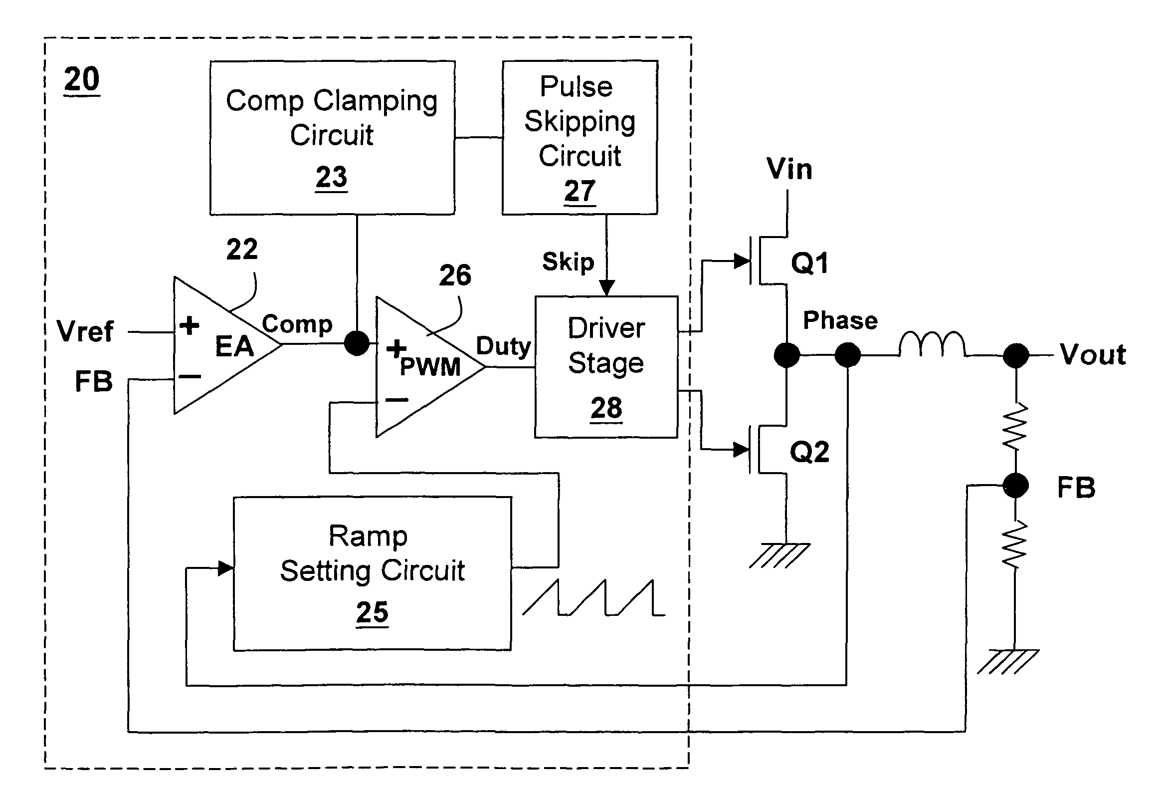
[0039]Referring to FIG. 9, the present invention is illustrated with a buck converter as an example. The switching regulator in this embodiment comprises a control circuit 20, which controls the operation of the power transistors Q1 and Q2 to convert electrical power from the input Vin to the output Vout. The control circuit 20 includes an error amplifier 22, a PWM comparator 26, a driver stage 28, an error amplification signal clamping circuit 23, a Ramp setting circuit 25 and a pulse skipping circuit 27. The error amplification signal clamping circuit (Comp clamping circuit) 23 determines the minimum level Comp_Min according to the level of the signal COMP in CCM or in a stable state. The Ramp setting circuit 25 is for generating a signal Ramp whose slope varies in accordance with the input voltage Vin. The Pulse skipping circuit 27 is for generating a pulse skipping signal Skip to trigger the pulse skipping mode.

[0040]The error amplification signal clamping circuit 23 and the Ram...

second embodiment

[0048]FIG. 15 shows the pulse skipping circuit 27. In the embodiment, a transistor 271 and the transistor 272 constitute a current mirror, which is another way to sense the current through the transistor 236. Similarly, when the current through the transistor 272 is higher than the current of the current source 273, the level of node B is high; when the current through the transistor 272 is lower than the current of the current source 273, the level of node B is low. In this embodiment, the signal at node B first passes through a hysteresis gate circuit 274, and then serves as the pulse skipping signal Skip; in this way, it can reduce noises in the signal and adjust the signal to an appropriate level.

third embodiment

[0049]FIG. 16 shows the pulse skipping circuit 27. In this embodiment, a delay circuit 275 is provided after the hysteresis gate circuit 274. The delay circuit 275 is to prevent the switching regulator from immediately switching to the pulse skipping mode when the signal Comp barely touches the minimum level Comp_Min, to prevent the signal Duty from being too short or unstable. With the delay circuit 275, the switching regulator enters the pulse skipping mode after the signal Comp reaches the minimum level Comp_Min for a period of time, or after at least one switching cycle of the power switches. The delay circuit 275 can be directly connected to the node B if no hysteresis gate circuit 274 is provided in the circuit.

[0050]An example of the delay circuit 275 is shown in FIG. 17, which is constituted by an SR flip-flop. The signal Duty is the clock input of the SR flip-flop, so that the pulse skipping signal Skip outputted from the SR flip-flop is delayed by one switching cycle of th...


PUM


Abstract

The present invention discloses a voltage mode switching regulator with improved light load efficiency and mode transition characteristic, and a control circuit and a control method therefor. The switching regulator can switch between a pulse width modulation (PWM) mode and a pulse skipping mode. The control method for the switching regulator comprises: comparing a feedback signal relating to an output voltage with a reference signal, to generate an error amplification signal; generating a duty signal according to the error amplification signal and a ramp signal, to control the switching regulator; setting a threshold level of the error amplification signal and a threshold level of the pulse skipping mode according to the error amplification signal in a stable status; and when the error amplification signal is close or equal to the threshold level of the pulse skipping mode, generating a pulse skip signal to enter the pulse skipping mode.

Description

BACKGROUND OF THE INVENTION[0001]1. Field of Invention[0002]The present invention relates to a switching regulator with improved light load efficiency and mode transition characteristic, and a control circuit and a control method therefor; particularly, it relates to a switching regulator capable of performing proper mode switching control without requiring an input voltage signal or an output voltage signal, and a control circuit and a control method therefor.[0003]2. Description of Related Art[0004]There are many types of switching regulators, such as buck converter, boost converter, inverter converter, and buck-boost converter, etc. The aforementioned regulators can also be divided into synchronous and asynchronous types. There are two (four for buck-boost converter) power transistor switches in the synchronous switching regulators, and one of the power transistor switches is replaced by a diode in the non-synchronous regulators. By way of example, FIG. 1 shows a synchronous buck...

Claims


Application Information

Patent Timeline
Patent Type & Authority Patents(United States)
IPC IPC(8): G05F1/40
CPCH02M3/1588H02M2001/0032Y02B70/1466Y02B70/16Y02B70/10H02M1/0032
Inventor CHEN, AN-TUNGWANG, JO-YU
Owner RICHTEK TECH
Why Eureka
Try Eureka