Solid-state image capturing apparatus and electronic information device

a technology of solid-state image and electronic information, which is applied in the direction of radio frequency controlled devices, instruments, television systems, etc., can solve the problems of failure to complete the transfer of signal charges generated in the light receiving section, and achieve the effect of convenient and stable transfer

Active Publication Date: 2012-09-11
SMARTSENS TECH (SHANGHAI) CO LTD
View PDF9 Cites 0 Cited by
  • Summary
  • Abstract
  • Description
  • Claims
  • Application Information

AI Technical Summary

Benefits of technology

[0037]The present invention is intended to solve the conventional problems described above. The objective of the present invention is to provide: a solid-state image capturing apparatus, in which an electric potential difference can be secured sufficiently between a photoelectric conversion element and a signal charge accumulation section when an electric potential of an FD is raised and a transferring transistor is turned on at a reset operation in a 3TR configuration pixel, the solid-state image capturing apparatus capable of facilitating complete transferring of signal charges from a photoelectric conversion element to a signal charge accumulation section as well as providing stable operations; and an electronic information device including the solid-state image capturing apparatus used therein.
[0052]According to the present invention, the solid-state image capturing apparatus includes a pixel array in which pixel sections are arranged in two dimensions, each pixel including at least: a photoelectric conversion element; a transferring transistor for transferring a signal charge from the photoelectric conversion element; a reset transistor for resetting an electric potential of an electric charge accumulation section; and an amplifying transistor for amplifying and reading out the electric potential of the electric charge accumulation section, source side of which is connected to a signal line. In the solid-state image capturing apparatus, a voltage supplying section is provided to supply a high voltage, which is higher than a power supply voltage, to a drain section of a reset transistor of the pixel array, thereby securing an electric potential difference sufficiently between a signal voltage and a reset voltage at the transferring of the signal charge and performing complete transferring of the signal charge from the photoelectric conversion element to an FD section easily and stably.
[0053]Further, according to the present invention, the high voltage supplying section is a charge pump circuit. Thus, the controlling of the operation of the charge pump circuit makes it possible to raise an electric potential supplied to the reset transistor of the pixel array to a desired electric potential.
[0054]Still further, according to the present invention, the reset transistor is a depletion type transistor. Thus, it becomes possible to prevent a reset voltage supplied through the reset transistor to a signal charge accumulation section from being lowered due to a threshold voltage of the reset transistor.
[0055]Still further, according to the present invention, a high voltage, which is higher than a power supply voltage, is applied to a gate electrode of the reset transistor, as to a reset drain section. Thus, it becomes possible to securely turn on the reset transistor in which an electric potential higher than the power supply voltage is supplied to a drain thereof.
[0056]Still further, according to the present invention, a constant current source is provided for each pixel column, the constant current source being connected to a read-out signal line of a corresponding pixel column. The constant current source is configured to include a MOS transistor connected between the read-out signal line and a ground, in which the MOS transistor operates to flow a constant current to the read-out signal line in a state where a pixel column corresponding to the read-out signal line is selected. Thus, it becomes possible to cut electricity that is consumed in the constant current source in a state where a pixel column corresponding to the read-out signal line is not selected.

Problems solved by technology

In the above method, however, due to the variation in response time required for the read-out signal line to follow the power supply voltage with respect to the reset pulse width, the difference in the response time of the read-out signal line depending on the position of the pixels, and the like, a problem of variation occurs in the reset electric potential of the FD section, resulting in failing the complete transferring of signal charges generated in the light receiving section.

Method used


Image

  • Solid-state image capturing apparatus and electronic information device
  • Solid-state image capturing apparatus and electronic information device
  • Solid-state image capturing apparatus and electronic information device

Examples


embodiment 1

[0090](Embodiment 1)

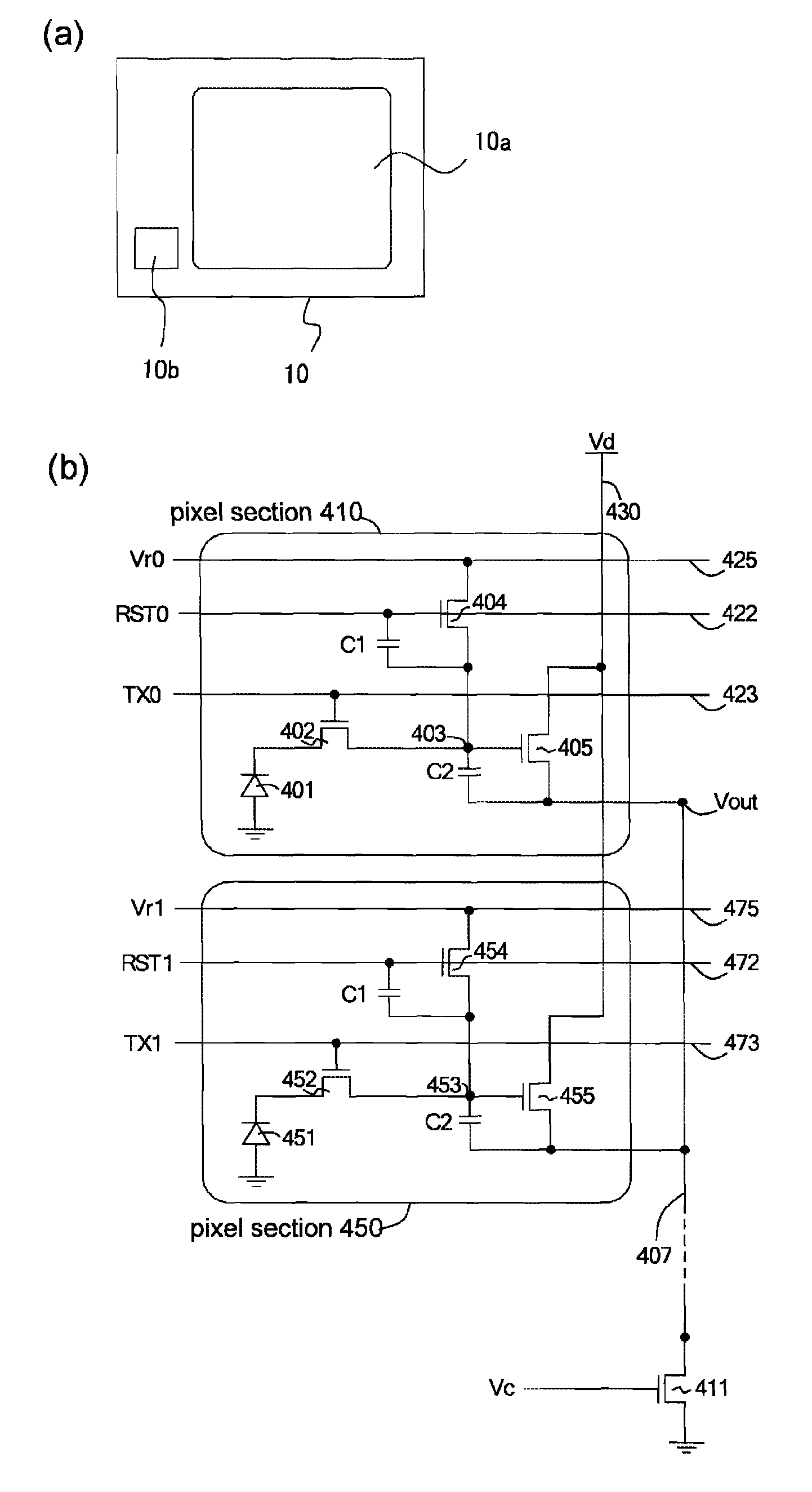
[0091]FIG. 1 is a diagram illustrating an amplification type solid-state image capturing apparatus according to Embodiment 1 of the present invention, FIG. 1(a) schematically illustrating an overall structure of the solid-state image capturing apparatus and FIG. 1(b) illustrating a circuit configuration of a 3TR configuration pixel in the solid-state image capturing apparatus.

[0092]An amplification type solid-state image capturing apparatus 10 according to Embodiment 1 includes a pixel array 10a in which 3TR configuration pixel sections (hereinafter, also referred to as pixel) are arranged in two dimensions; and a controlling section 10b disposed in the periphery of the pixel array 10a for controlling the pixel array 10a.

[0093]As similar to a conventional pixel, a 3TR configuration pixel section 410 in the amplification type solid-state image capturing apparatus 10 includes: alight receiving section 401 for converting light to electrons; a transferring transisto...

embodiment 2

[0120](Embodiment 2)

[0121]FIG. 4 is a block diagram schematically illustrating an exemplary configuration of an electronic information device, as Embodiment 2 of the present invention, including the solid-state image capturing apparatus according to Embodiment 1 of the present invention used in an image capturing section thereof.

[0122]The electronic information device 90 according to Embodiment 2 of the present invention as illustrated in FIG. 4 includes the solid-state image capturing apparatus according to Embodiment 1 of the present invention as an image capturing section 91 for capturing a subject. The electronic information device 90 further includes at least any of: a memory section 92 (e.g., recording media) for data-recording a high-quality image data obtained by an image capturing section after a predetermined signal process is performed on the image data for recording; a display section 93 (e.g., liquid crystal display device) for displaying this image data on a display sc...


PUM


Abstract

In a three-TR configuration pixel, the solid-state image capturing apparatus according to the present invention is capable of securing an electric potential difference sufficiently between a signal voltage and a reset voltage at the transferring of a signal charge and performing complete transferring of the signal charge from a photoelectric conversion element to an FD section easily and stably. Each pixel section, constituting a pixel array, has a 3TR configuration including reset transistors, transfer transistors and amplifying transistors. In each row of the pixel array, provided are a level shifter for driving reset drain wiring connected to a drain of the reset transistor, with an electric potential higher than a power supply voltage, and another level shifter for driving a reset signal line connected to a gate of the reset transistor, with an electric potential higher than the power supply voltage.

Description

[0001]This nonprovisional application claims priority under 35 U.S.C. §119(a) to Patent Application No. 2009-123632 filed in Japan on May 21, 2009, the entire contents of which are hereby incorporated by reference.BACKGROUND OF THE INVENTION[0002]1. Field of the Invention[0003]The present invention relates to a solid-state image capturing apparatus and an electronic information device, and more particularly, to an amplification type solid-state image capturing apparatus, in which a pixel section includes an amplifier circuit, with improved performance, and an electronic information device including the amplification type solid-state image capturing apparatus used therein.[0004]2. Description of the Related Art[0005]Typically, a common amplification type solid-state image capturing apparatus includes a pixel array section in which pixel sections (also referred to simply as pixel) with amplification function are arranged in two dimensions, and a scanning circuit disposed in the periph...

Claims


Application Information

Patent Timeline
Patent Type & Authority Patents(United States)
IPC IPC(8): H04N5/335H04N3/14H01L27/00H01L27/146H04N5/357H04N5/369H04N5/374
CPCH04N5/335H04N5/3597H04N25/00H04N25/626
Inventor MORIMOTO, HIDENORI
Owner SMARTSENS TECH (SHANGHAI) CO LTD
Why Eureka
Try Eureka