Load lock design for rapid wafer heating

a technology of loading lock and wafer, which is applied in the direction of electrostatic spraying apparatus, spraying apparatus, electrical apparatus, etc., can solve the problems of inefficient wafer heating, particle contamination of wafers, load locks that do not have in situ cleaning capability, etc., and achieve uniform and rapid heating and improve throughput

Active Publication Date: 2012-09-25
NOVELLUS SYSTEMS
View PDF82 Cites 19 Cited by
  • Summary
  • Abstract
  • Description
  • Claims
  • Application Information

AI Technical Summary

Benefits of technology

[0011]The present invention provides a wafer heating process and apparatus for uniform and rapid heating in a changing pressure environment, such as a load lock. In accordance with the invention, a semiconductor processing tool heats wafers in a load lock using a radiant heat source and a resistive heat source. The wafers are heated in greater part with a resistive heat source until a transition temperature or pressure is reached, then they are heated in greater part with a radiant heat source. Throughput improves for the tool because the wafers can uniformly reach a high temperature in seconds.

Problems solved by technology
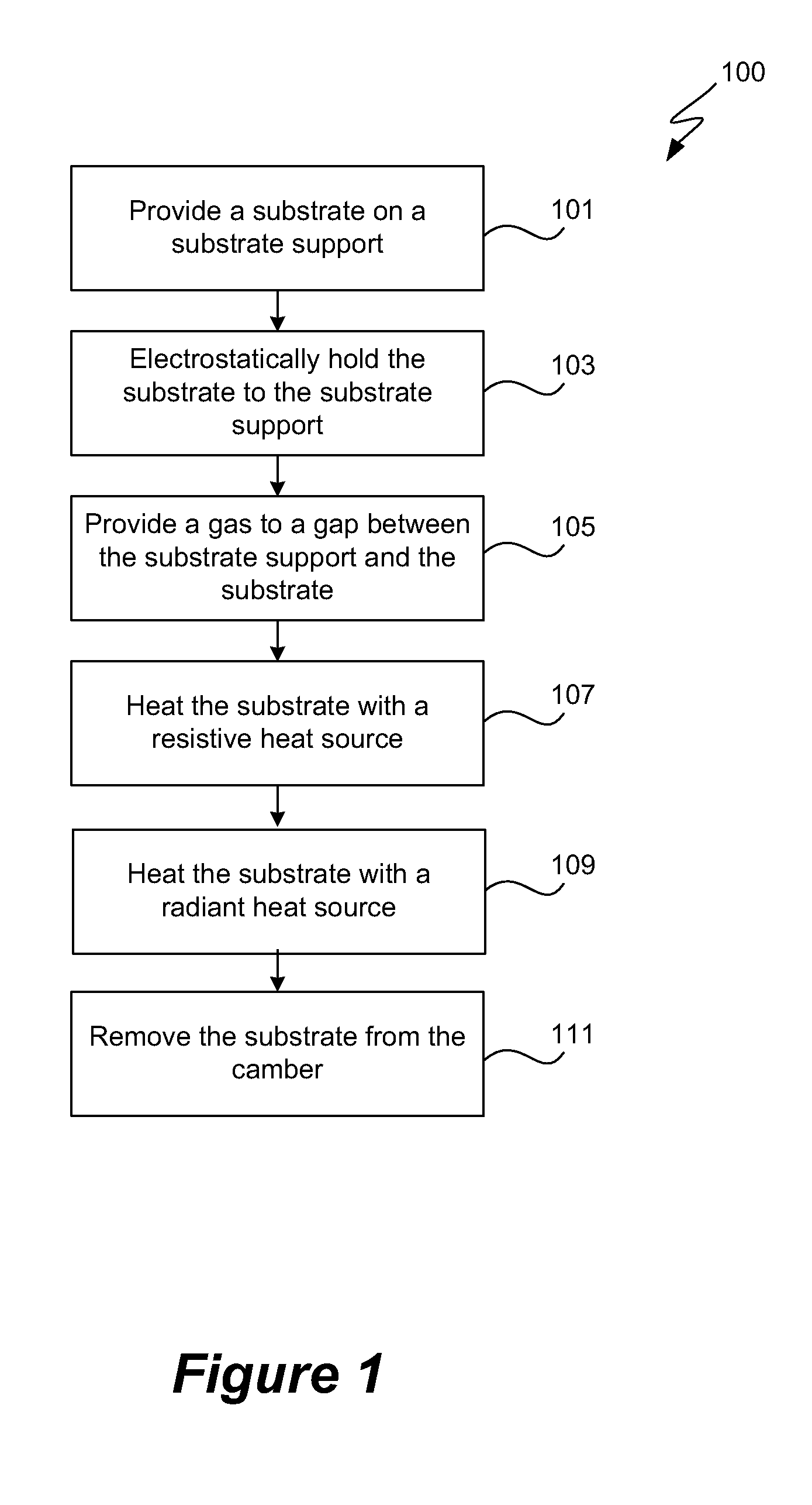
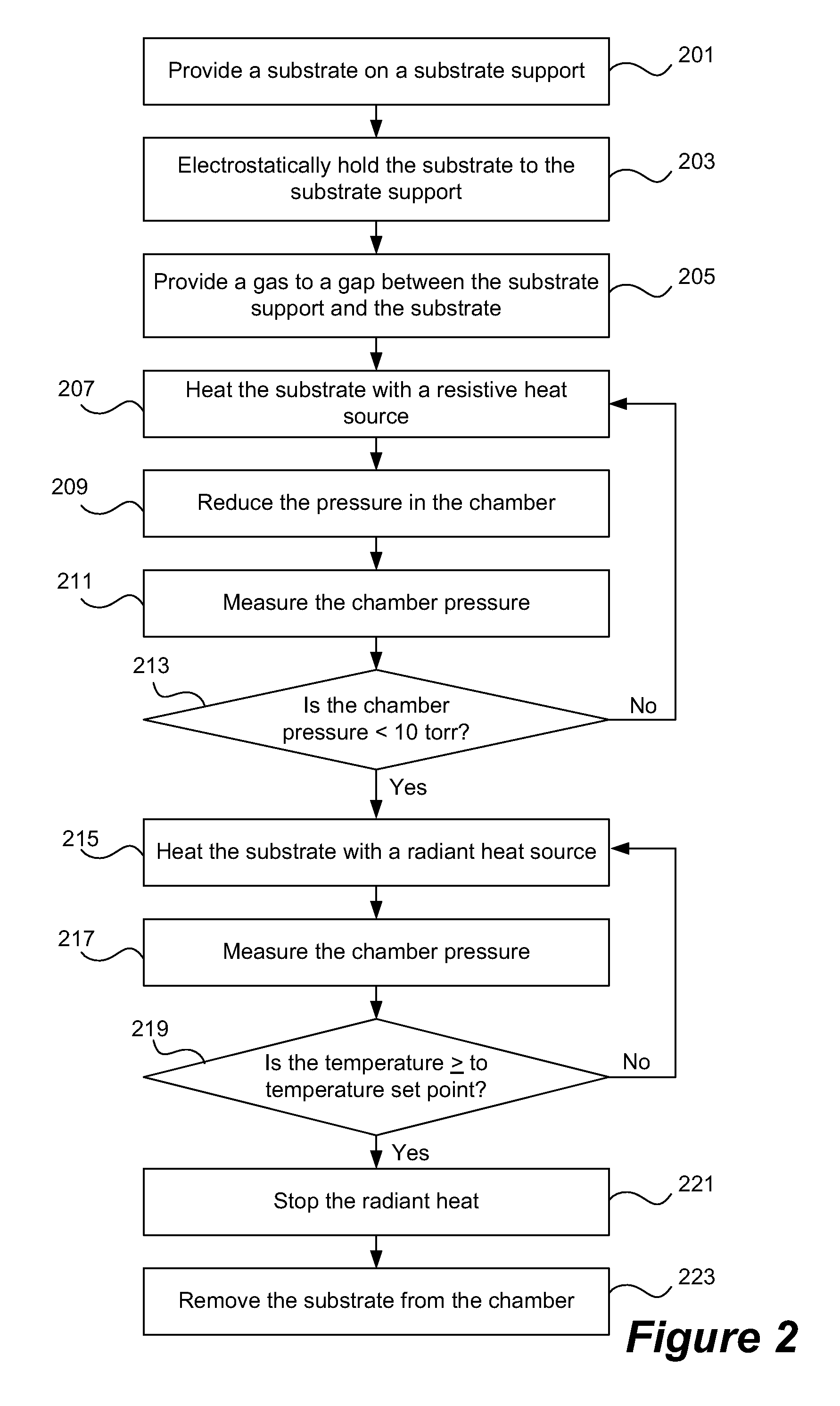
Particles that can contaminate a wafer may be generated by the chemical or physical processes in the process chamber, scraping of wafer handling components, or chemical incompatibilities of the different materials.
Additionally, load locks are not equipped with in situ cleaning capability.
But this wafer heating is inefficient because the pedestal has to be maintained at a much higher temperature than the desired wafer temperature.
Maintaining a high pedestal temperature limits the types of materials that may be used and the life of the pedestal.
Further, having such a high temperature object in close proximity to the wafer interferes with wafer temperature measurement for temperature control.
This technique of heating a wafer in a load lock is also slow.
The heating time required to reach a steady-state temperature may be longer than the processing time in a process station, making the load lock pre-heat the throughput limiting process step, reducing tool throughput for some applications.
An alternative is to remove a wafer before a steady-state temperature is reached, but because wafer temperature cannot be accurately measured, the downstream semiconductor process may be affected adversely if the wafer is too hot or too cold or if the temperature is not uniform across the wafer.

Method used


Image

  • Load lock design for rapid wafer heating
  • Load lock design for rapid wafer heating
  • Load lock design for rapid wafer heating

Examples


Embodiment Construction

[0024]In the following detailed description of the present invention, a number of specific embodiments are set forth in order to provide a thorough understanding of the invention. However, as will be apparent to those skilled in the art, the present invention may be practiced without these specific details or by using alternate elements or processes. In some descriptions herein, well-known processes, procedures, and components have not been described in detail so as not to unnecessarily obscure aspects of the present invention.

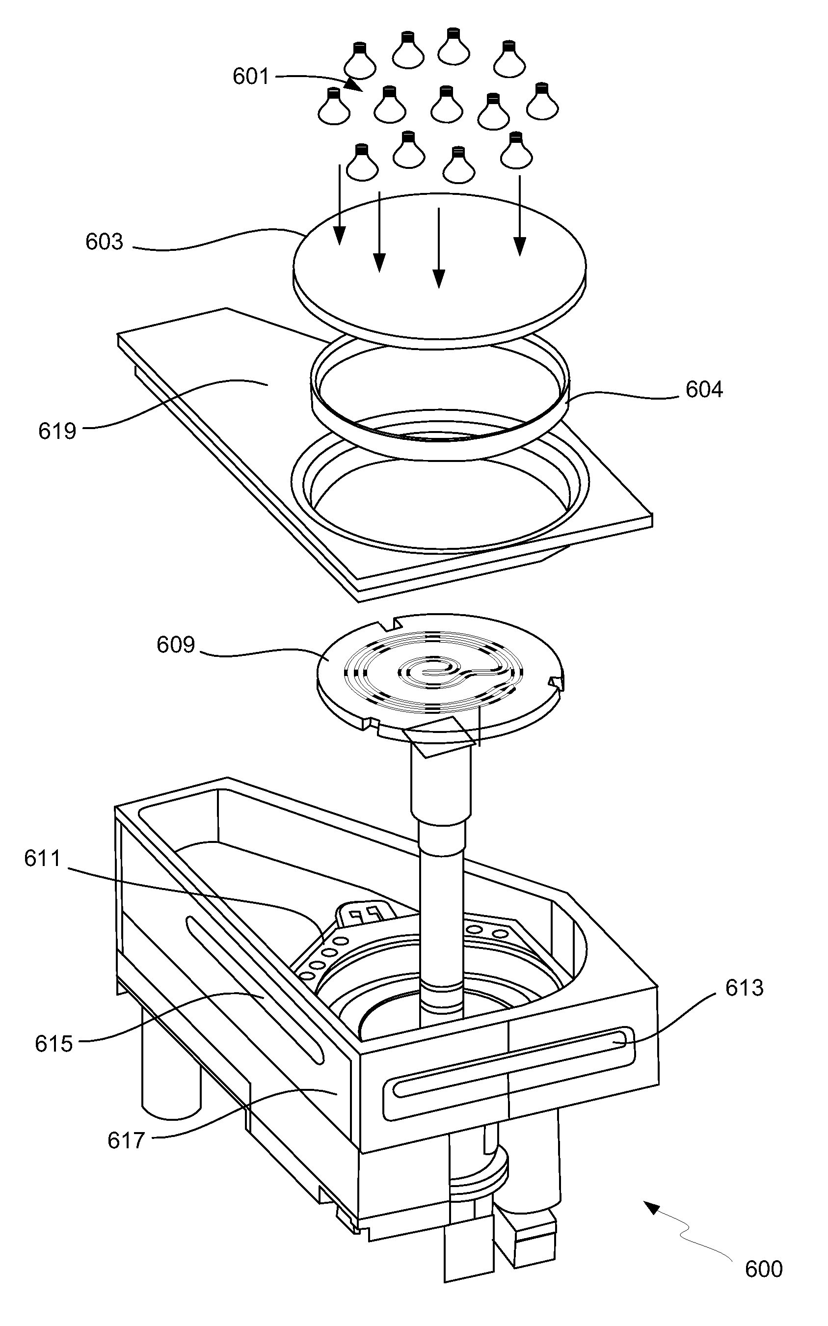
[0025]In this application, the terms “wafer” and “substrate” and terms “substrate support” and “pedestal” will be used interchangeably. The following detailed description assumes the invention is implemented on a wafer. However, the invention is not so limited. The work piece may be of various shapes, sizes, and materials. In addition to semiconductor wafers, other work pieces that may take advantage of this invention include various articles such as display b...


PUM


Abstract

A semiconductor processing tool heats wafers using radiant heat and resistive heat in chamber or in a load lock where pressure changes. The wafers are heated in greater part with a resistive heat source until a transition temperature or pressure is reached, then they are heated in greater part with a radiant heat source. Throughput improves for the tool because of the wafers can reach a high temperature uniformly in seconds.

Description

CROSS REFERENCE TO RELATED APPLICATION[0001]This application is a continuation of prior application Ser. No. 11 / 608,185 filed on Dec. 7, 2006, now pending, the disclosure of which is incorporated by reference herein in its entirety.FIELD OF THE INVENTION[0002]The present invention relates generally to semiconductor device fabrication, and more particularly to semiconductor wafer processing systems. Even more specifically, it relates to methods and apparatus for heating a wafer.BACKGROUND OF THE INVENTION[0003]A typical semiconductor wafer processing system has a process chamber for processing semiconductor wafers and wafer handling modules for moving the wafers in and out of the process chamber. Process chambers are available for chemical vapor deposition, physical vapor deposition, etching, electro-plating / electro-fill, plasma, thermal and radiation treatments, and other semiconductor device fabrication processes. For example, a chemical vapor deposition chamber may be used to depo...

Claims


Application Information

Patent Timeline
Patent Type & Authority Patents(United States)
IPC IPC(8): H01L21/00B05B5/00
CPCH01L21/67103H01L21/67115H01L21/67248
Inventor RIVKIN, MICHAELPOWELL, RONHAMILTON, SHAWNNORDIN, MICHAEL
Owner NOVELLUS SYSTEMS
Why Eureka
Try Eureka