

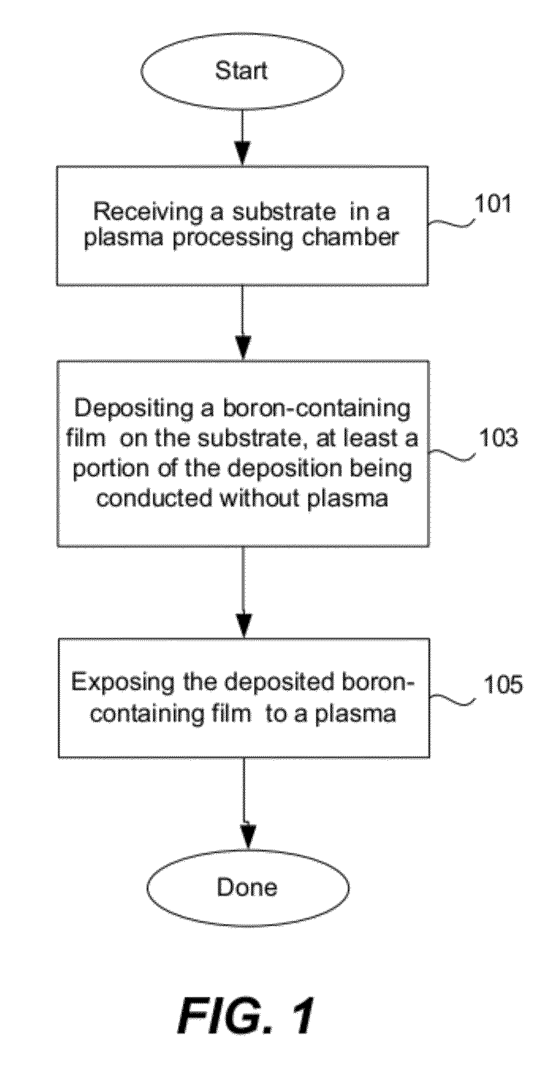
Depositing conformal boron nitride film by CVD without plasma
a boron nitride film and conformal technology, applied in the field of electromechanical devices, can solve the problems of pattern loading effect on the conformality of these materials, and achieve the effect of low dielectric constant and low wet etch ra
- Summary
- Abstract
- Description
- Claims
- Application Information
AI Technical Summary
Benefits of technology
Problems solved by technology
Method used
Image

Examples
examples
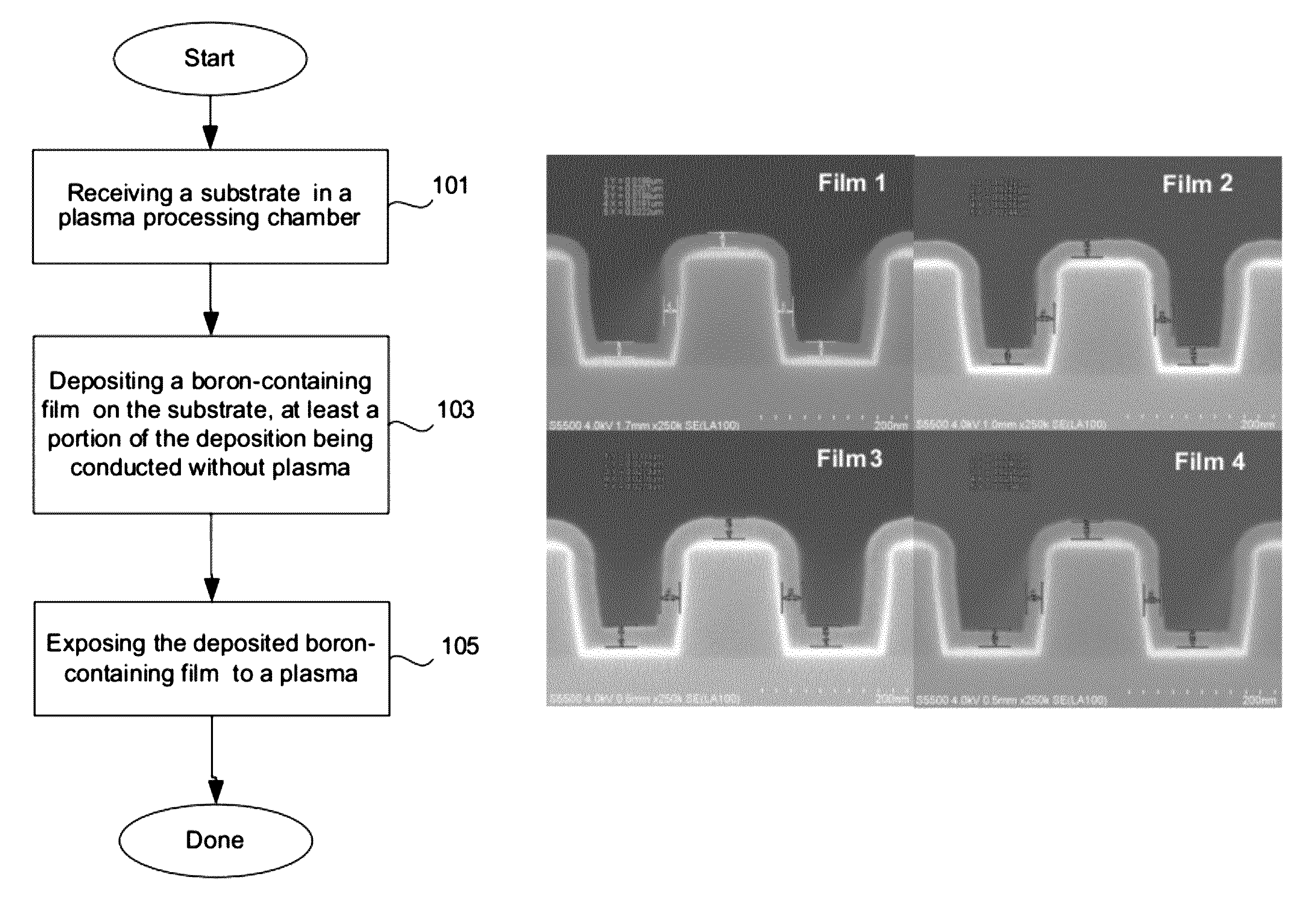
[0053]The following examples are provided to further illustrate aspects and advantages of the present invention. These examples are provided to exemplify and more clearly illustrate aspects of the present invention and are in no way intended to be limiting.
[0054]Several dielectric layers were formed by boron nitride film deposition and treatment in accordance with the present invention. Process parameters and details is are noted in Table 1, below:
[0055]
TABLE 1B2H6 Soak ConditionsPreSDPost Treat ConditionsFilmtreatB2H6NH3H2HeTimePurgeNH3N2HFRFLFRFTimeFilm 1—412570000015—7000 0005Film 2—412570000015With700007504505NH3Film 3—41257000005With7000075045010NH3Film 4UV41257000005With7000075045010SiNNH31 secFilm 5—41257000005With7000075045020NH3Film 6—41257000005With7001500075045010NH3
[0056]Film 1 was made by CVD boron nitride without post-deposition plasma treatment for purposes of comparison with Films 2-6 formed in accordance with the present invention. The remaining films were conformal...
PUM
| Property | Measurement | Unit |
|---|---|---|
| temperature | aaaaa | aaaaa |
| flow rate | aaaaa | aaaaa |
| power | aaaaa | aaaaa |
Abstract
Description
Claims
Application Information