Reduced swing differential pre-drive circuit

a differential pre-drive and voltage reduction technology, applied in the direction of differential amplifiers, amplifiers with semiconductor devices/discharge tubes, instruments, etc., can solve the problems of difficulty in obtaining up to hdtv formats (19201080) on display sizes beyond 50 inches, and the maximum operating frequency of conventional transmitter designs is limited, so as to reduce the voltage swing of the differential pair of input signals, and reduce the swing and offset

Active Publication Date: 2012-10-16
NAT SEMICON CORP
View PDF4 Cites 8 Cited by
  • Summary
  • Abstract
  • Description
  • Claims
  • Application Information

AI Technical Summary

Benefits of technology

[0008]Specifically, in one embodiment, a circuit for reducing and offsetting the voltage swing of a differential pre-drive circuit is described. The circuit comprises a first H-bridge of transistors receiving a differential pair of input signals. A swing resister is coupled to the H-bridge for reducing a voltage swing of the differential pair of input signals. The reduced swing is exhibited within a differential pair of output signals. Also, the differential pre-drive circuit includes an offset resistor that is coupled to the H-bridge. The offset resistor acts to offset the differential pair of output signals. As such, the differential pair of output signals, having reduced swing and offset, as applied to gates of output transistors in an output stage allow the output transistors to remain in or near the saturation operating state.
[0009]In another embodiment, a transmitter of a timing controller communicating over a point-to-point differential signaling (PPDS) data channel is described. The transmitter includes a complementary-symmetry (CMOS) buffer stage providing a differential pair of input signals. The transmitter also comprises a differential pre-drive circuit that is capable of reducing a voltage swing of the differential pair of input signals as generated as a differential pair of output signals. Additionally, the differential pre-drive circuit is capable of offsetting the differential pair of output signals. The transmitter also comprises an output stage that receives the differential pair of output signals. The differential pair of output signals, having reduced swing and offset, as applied to gates of output transistors in an output stage allow the output transistors to remain in or near the saturation operating state resulting in higher switching frequencies and cleaner output waveforms.

Problems solved by technology

However, pushing LCDs to the next generation by simply scaling existing LCD monitor panels to wider formats (e.g., 16:9 HDTV) and larger formats is a complicated endeavor.
Specifically, LCD televisions bring forward a completely new set of challenges that are broader than simple data signaling issues.
The demand for up to HDTV formats (1920×1080) on display sizes beyond 50 inches are problematic.
In particular, conventional transmitter designs have limited maximum operating frequencies and less than ideal output waveforms exhibiting overshoot and undershoot disturbances.
As a result, this type of pre-drive limits the maximum frequency of the transmitter and correspondingly the data channel.
This limitation occurs since it takes time to charge and discharge the channels of the output transistors.
In addition, this type of pre-drive creates glitches in the output waveform because the channels of the transistors in the output stage are completely charged and discharged as they leave and re-enter the saturated operating mode.

Method used


Image

  • Reduced swing differential pre-drive circuit
  • Reduced swing differential pre-drive circuit
  • Reduced swing differential pre-drive circuit

Examples


Embodiment Construction

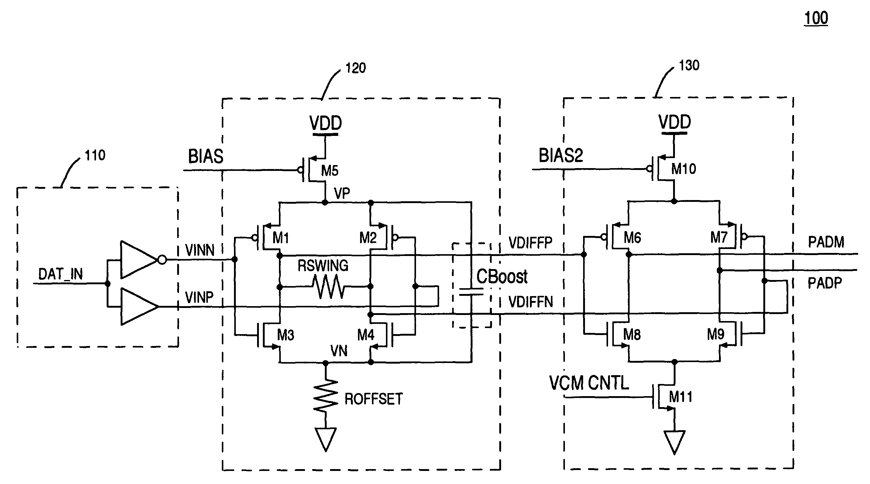
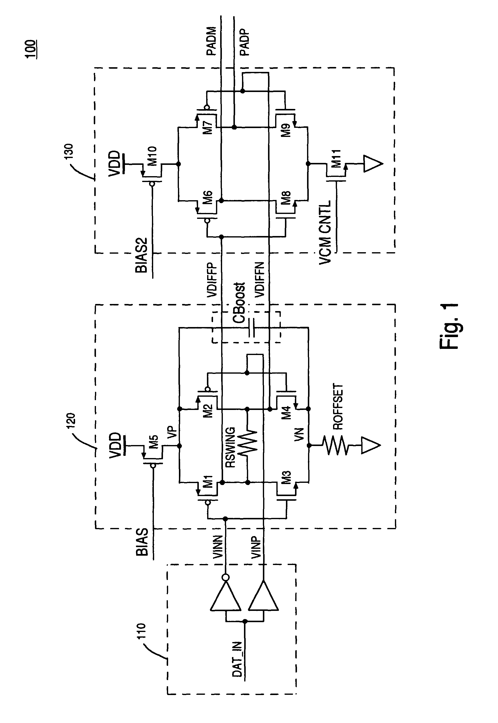
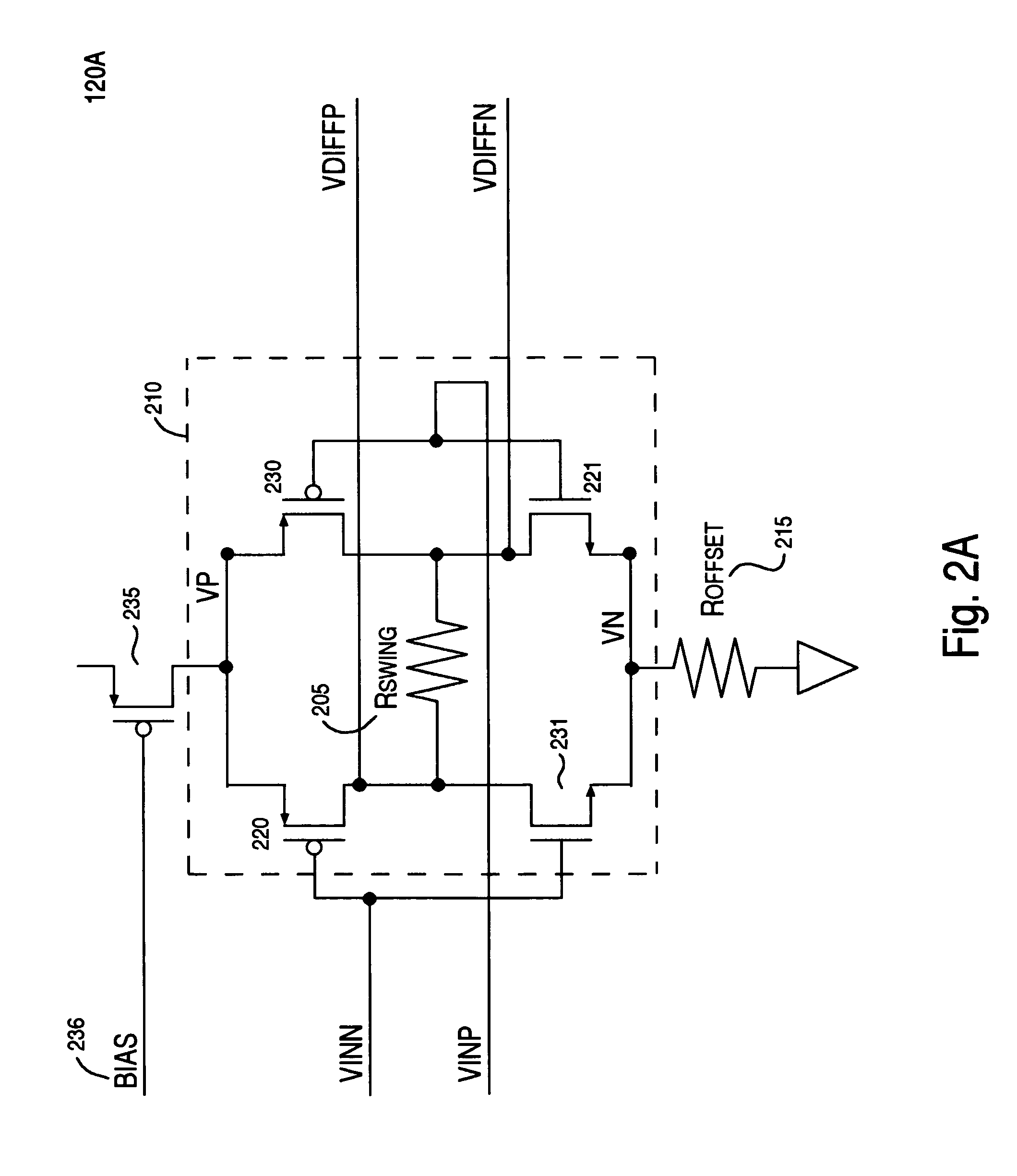
[0017]Reference will now be made in detail to the preferred embodiments of the present invention, a reduced swing with offset differential pre-drive circuit, examples of which are illustrated in the accompanying drawings.

[0018]Accordingly, various embodiments of the present invention disclose a pre-drive circuit with reduced swing and offset. Embodiments of the present invention are capable of achieving higher operating frequencies with lower power requirements over conventional transmitter designs. In addition, embodiments of the present invention describe transistors in an output stage that are driven by a reduced swing and offset pre-drive circuit that exhibits output waveforms that do not exhibit glitches (e.g., overshoot and undershoot disturbances) due to capacitive coupling.

[0019]The following detailed description is of example embodiments of the presently claimed invention with references to the accompanying drawings. Such description is intended to be illustrative and not l...


PUM


Abstract

A circuit for reducing and offsetting the voltage swing of a differential pre-drive circuit. The circuit includes a first H-bridge of transistors receiving a differential pair of input signals. A swing resister is coupled to the H-bridge for reducing a voltage swing of the differential pair of input signals. The reduced swing is generated as a differential pair of output signals. Also, the differential pre-drive circuit includes an offset resistor that is coupled to the H-bridge. The offset resistor acts to offset the differential pair of output signals. As such, the differential pair of output signals having reduced swing and offset as applied to gates of output transistors in an output stage allow the output transistors to remain in the saturation operating state.

Description

BACKGROUND OF THE INVENTION[0001]1. Field of the Invention[0002]Embodiments of the present invention relate to the field of timing controllers. More particularly, embodiments of the present invention relate generally to a differential pre-drive circuit exhibiting reduced swing and offset.[0003]2. Related Art[0004]Liquid crystal displays (LCDs) are important to the television market. However, pushing LCDs to the next generation by simply scaling existing LCD monitor panels to wider formats (e.g., 16:9 HDTV) and larger formats is a complicated endeavor. A number of television requirements push beyond conventional state-of-the art monitors. For instance, response time, brightness, contrast, color envelope, color temperature, and progressive scan-and-hold issues require a re-engineering of the monitor solution.[0005]Specifically, LCD televisions bring forward a completely new set of challenges that are broader than simple data signaling issues. The demand for up to HDTV formats (1920×10...

Claims


Application Information

Patent Timeline
Patent Type & Authority Patents(United States)
IPC IPC(8): G09G3/36
CPCG09G3/3611G09G2370/08G09G2370/14
Inventor SIMON, DANIEL L.
Owner NAT SEMICON CORP
Why Eureka
Try Eureka