Method of manufacturing semiconductor device, and bonding apparatus

a technology of semiconductor devices and bonding apparatus, which is applied in the direction of soldering apparatus, manufacturing tools,auxillary welding devices, etc., can solve the problems of inability to reduce the pitch of the pad surface between adjacent pad surfaces, inability to accurately bond onto the small pad surface, and inability to stabilize the substrate, so as to improve the accuracy of bonding and reduce the deformation area , the effect of reliably cutting

Active Publication Date: 2012-10-23
SHINKAWA CO LTD
View PDF25 Cites 10 Cited by
  • Summary
  • Abstract
  • Description
  • Claims
  • Application Information

AI Technical Summary

Benefits of technology

[0009]It is hence an object of the present invention to provide a method of manufacturing a semiconductor device and a bonding apparatus with which an initial ball, when bonded to a pad surface of the semiconductor device, can have a small deformation area for improvement in the accuracy of bonding. It is another object of the present invention to provide a method of manufacturing a semiconductor device and a bonding apparatus with which a bonding wire, when bonded to a lead surface of a substrate, can be cut reliably.

Problems solved by technology

However, the substrate may be in an unstable state such as wobbling on a bonding stage, suffering from a problem in that the initial ball may not be bonded reliably to the pad surface in the first bonding step and / or the bonding wire may not be cut in the second bonding step.
For this reason, the related art described in Japanese Patent No. 2530224 suffers from a problem in that accurate bonding onto a small pad surface is difficult and the pad pitch serving as the distance between adjacent pad surfaces, cannot be reduced.

Method used


Image

  • Method of manufacturing semiconductor device, and bonding apparatus
  • Method of manufacturing semiconductor device, and bonding apparatus
  • Method of manufacturing semiconductor device, and bonding apparatus

Examples


first exemplary embodiment

[First Exemplary Embodiment]

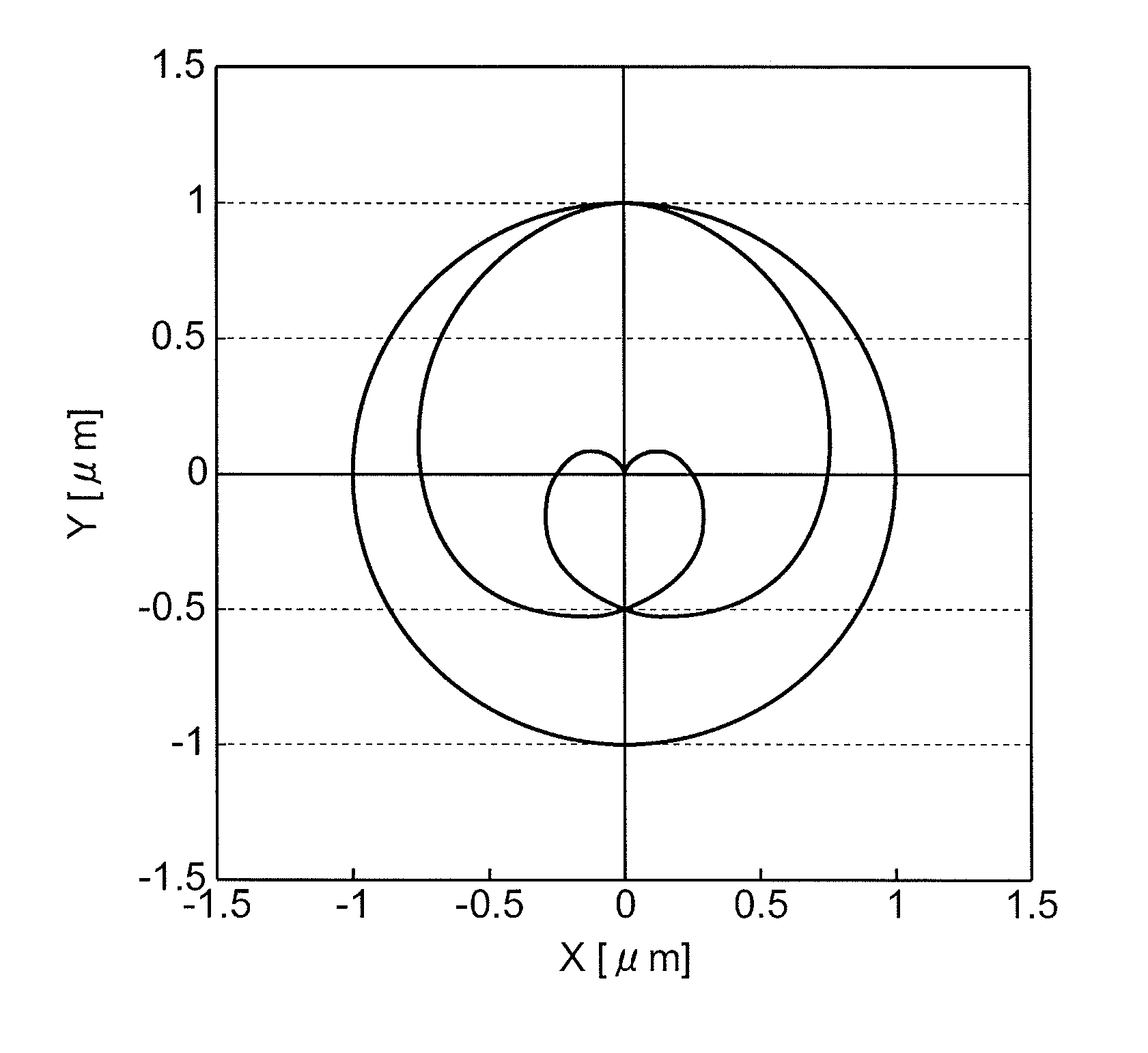
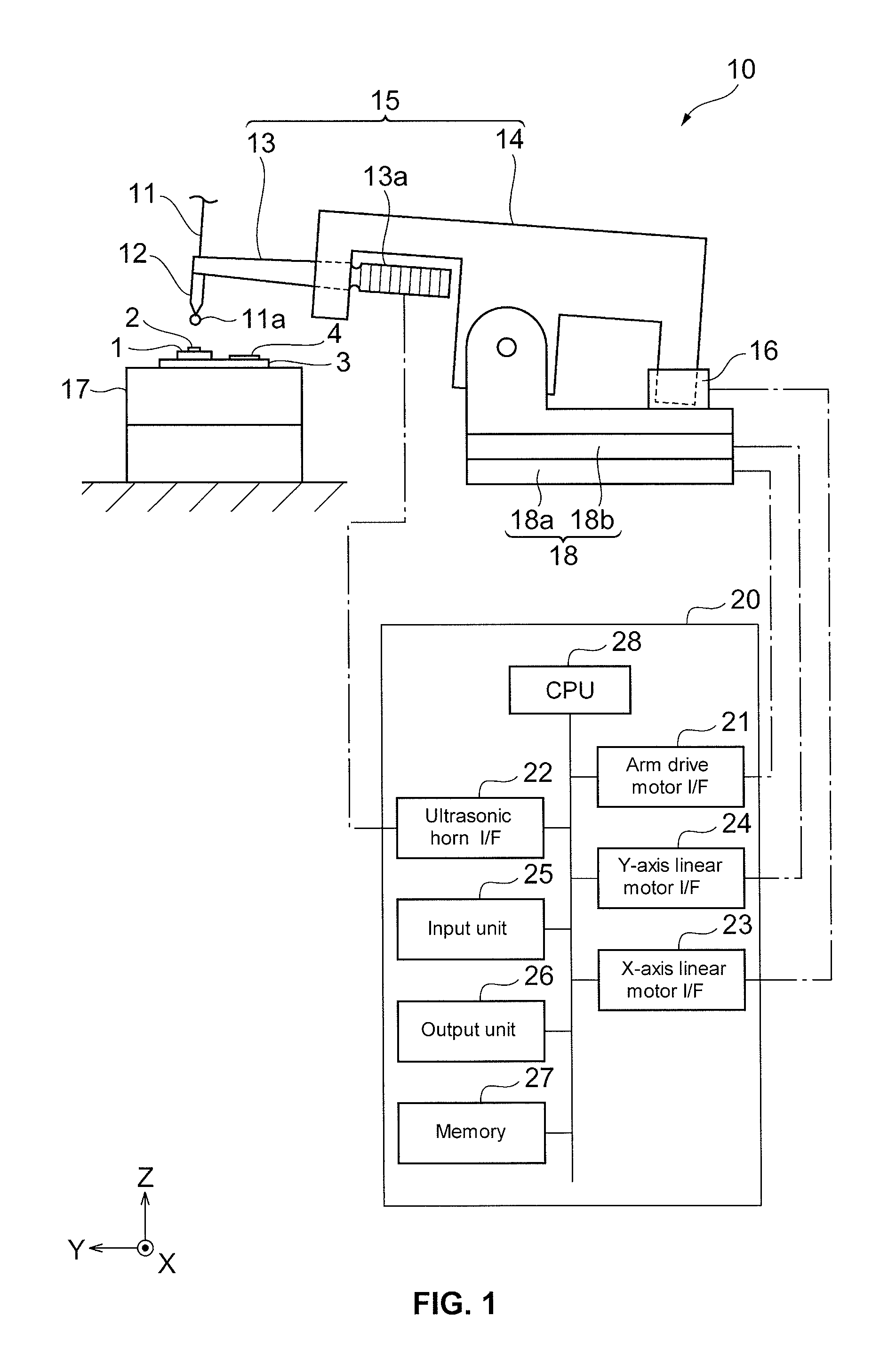
[0045]FIG. 1 illustrates an example of a wire-bonding apparatus according to a first exemplary embodiment. As shown in FIG. 1, the wire-bonding apparatus 10 according to the first exemplary embodiment is configured to electrically connect a pad surface 2 provided on a semiconductor device 1 and a lead surface 4 provided on a substrate 3 on which the semiconductor device 1 is bonded, through wire bonding using a bonding wire 11 inserted through a capillary 12. The wire-bonding apparatus 10 thus includes the capillary 12 through which the bonding wire 11 is inserted, a bonding head 15 for holding the capillary 12, an arm drive motor 16 for rotating (swinging) the bonding head 15, a bonding stage 17 on which the substrate 3 is placed as a bonding target, an XY movement mechanism 18 for moving the bonding head 15 horizontally in X- and Y-axis directions, and a control unit 20 for integrally controlling the wire-bonding apparatus 10.

[0046]The bonding head 15 i...

second exemplary embodiment

[Second Exemplary Embodiment]

[0073]FIG. 9 illustrates an example of a bump-bonding apparatus according to a second exemplary embodiment. As shown in FIG. 9, the bump-bonding apparatus 30 according to the second exemplary embodiment is configured to form a bump on a pad surface 8 formed on each of one or more semiconductor devices 7 that are bonded to a substrate 6, through bonding of a bonding wire 11 inserted through a capillary 12. The bump-bonding apparatus 30 basically has the same configuration as the wire-bonding apparatus 10 according to the first exemplary embodiment, though different in the bonding target and bonding method. Like the wire-bonding apparatus 10, the bump-bonding apparatus 30 thus includes the capillary 12 through which the bonding wire 11 is inserted, a bonding head 15 for holding the capillary 12, an arm drive motor 16 for rotating (swinging) the bonding head 15, a bonding stage 17 on which the substrate 6 is placed as a bonding target, an XY movement mechan...


PUM

PropertyMeasurementUnit
diameteraaaaaaaaaa
pressureaaaaaaaaaa
diameteraaaaaaaaaa

Abstract

In a first bonding step of bonding an initial ball to a pad surface, the initial ball is applied by ultrasonic vibration while in pressure contact with the pad surface and a capillary undergoes a scrubbing motion to be rotated spirally. This allows a deformation area of the initial ball to be reduced, whereby the accuracy of bonding can be improved. In a second bonding step of bonding a bonding wire to a lead surface, the capillary and the bonding wire are applied by ultrasonic vibration while in pressure contact with the lead surface and the capillary undergoes a scrubbing motion to be rotated spirally. This allows the bonding wire bonded to the lead surface to be cut reliably.

Description

BACKGROUND OF THE INVENTION[0001]1. Field of the Invention[0002]The present invention relates to a method for manufacturing a semiconductor device including bonding onto a bonding target, and to bonding apparatuses.[0003]2. Description of the Related Art[0004]Wire-bonding generally includes a first bonding step in which an initial ball is formed at a tip end of a bonding wire to be fed out of a capillary and is applied by ultrasonic vibration while in pressure contact with a pad surface of a semiconductor device to bond the initial ball to the pad surface. In a second bonding step thereafter, the bonding wire is fed out of the capillary to form a wire loop, and the bonding wire and the capillary are brought into pressure contact with a lead surface of a substrate to bond the bonding wire to the lead surface and then cut the bonding wire.[0005]However, the substrate may be in an unstable state such as wobbling on a bonding stage, suffering from a problem in that the initial ball may ...

Claims


Application Information

Patent Timeline
Patent Type & Authority Patents(United States)
IPC IPC(8): B23K31/02
CPCB23K20/007B23K20/10H01L24/49H01L24/78H01L24/85H01L2924/01033H01L2924/01006H01L2924/01082H01L2924/01005H01L2924/01004H01L2224/85205H01L2224/85181H01L2224/85045H01L2224/78901H01L2224/78823H01L2224/78801H01L2224/78301H01L2224/48225H01L2224/48247H01L2224/48463H01L2224/49171H01L2224/78268H01L2924/00014H01L2924/00H01L2224/48227H01L24/48H01L2224/45099H01L2224/05599
Inventor MARUYA, YUSUKEAOYAGI, NOBUYUKI
Owner SHINKAWA CO LTD
Why Eureka
Try Eureka