Supercharge Your Innovation With Domain-Expert AI Agents!

Photovoltaic cells based on nano or micro-scale structures

a photovoltaic cell and nano- or micro-scale technology, applied in the direction of solid-state devices, electrical devices, semiconductor devices, etc., can solve the problems of reducing the conversion efficiency, the toxic nature of these materials is of great concern to the environment, so as to achieve the effect of increasing the power generation capacity

Active Publication Date: 2012-11-20
BANPIL PHOTONICS
View PDF13 Cites 1 Cited by
  • Summary
  • Abstract
  • Description
  • Claims
  • Application Information

AI Technical Summary

Benefits of technology

"The invention provides structures of photovoltaic cells that have high power generation capability per unit area, compared to conventional counterparts. It reduces the recombination of carriers and increases the absorption of light, which leads to an increase in photogenerated carriers. The invention also provides solar cell structures based on nano or micro scaled-blocks, such as rods, wires, or tubes, which can be formed on a base substrate such as Si, Ge, or glass, to decrease the cost. The invention can capture most of the wavelengths belonging to the solar spectrum and provide high conversion efficiency. It can generate electric power when the sun is out and is not out. The invention offers the advantage of achieving high conversion efficiency using Si-materials and other materials."

Problems solved by technology

Although the fabrication processes of amorphous silicon based photovoltaic cells are rather simple and inexpensive, one notable downside of this type of cell is its vulnerability to defect-induced degradation that decreases its conversion efficiency.
This conversion efficiency is comparable to those for the single crystalline silicon photovoltaic devises; however, the toxic nature of these materials is of great concern for environment.
], which again raises issues associated with the toxic nature of these materials.
In general, synthesis processes of single crystalline group III-V are very costly because of substantial complications involved in epitaxial growth of group III-V single crystalline compound semiconductors.
Thus, the basic structure of current photovoltaic cells has its own limitation on increasing the conversion efficiency.
Today's photovoltaic cells are structured in such a way that (a) wide ranges of the solar spectrum cannot be absorbed due to material limitations, and (b) PCCE is low due to its inherent structure.
Additionally, today's solar cell material is not highly radiation-tolerant.

Method used


Image

  • Photovoltaic cells based on nano or micro-scale structures
  • Photovoltaic cells based on nano or micro-scale structures
  • Photovoltaic cells based on nano or micro-scale structures

Examples


Embodiment Construction

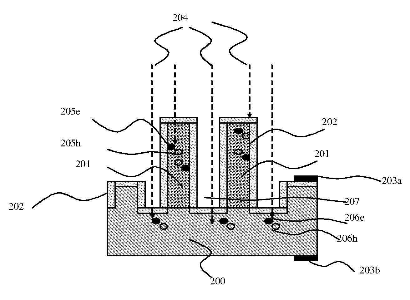
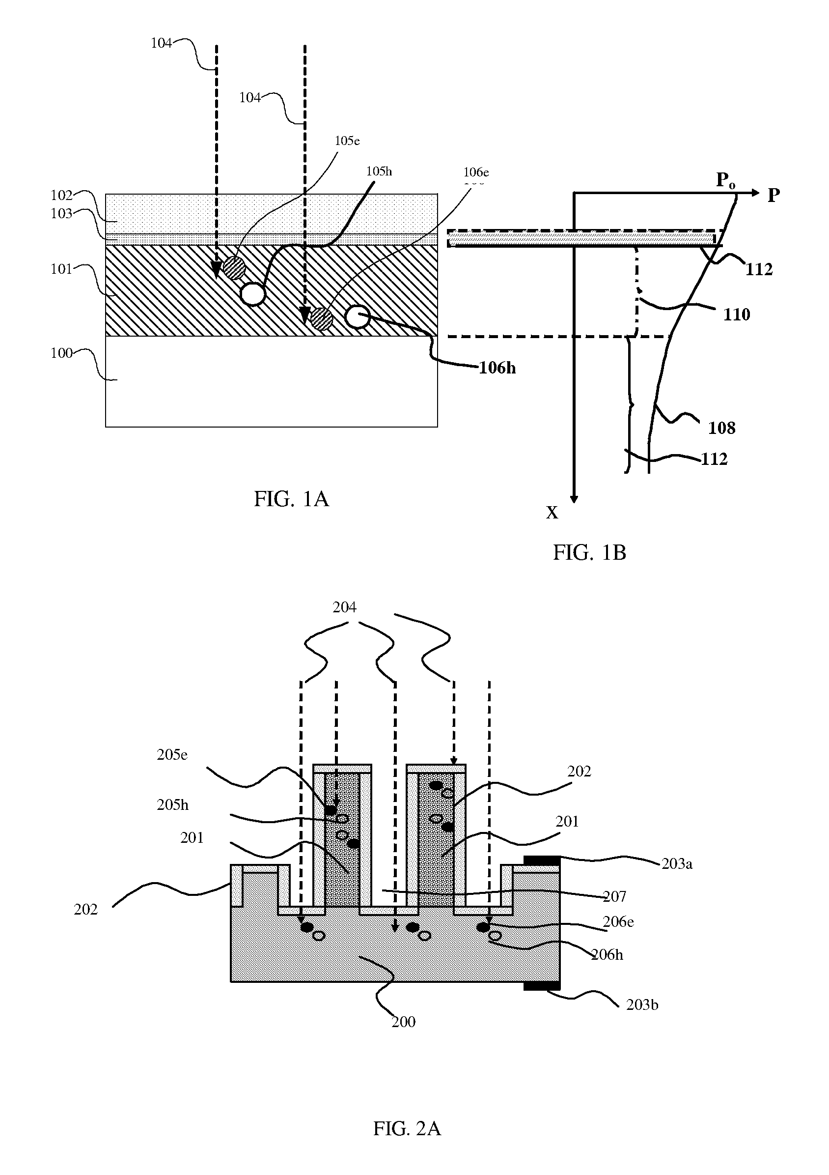
[0033]According to the preferred embodiment illustrated in FIG. 2A, a photovoltaic cell comprising of a plurality of nanometer(s) or micrometer(s)-scaled rods 201 is formed on the supporting substrate 200 (after having groove). The nanometer(s) or micrometer(s)-scaled rods 201 can have metallic electrical conduction, p-type or n-type semiconductor electrical conduction. The nanometer(s) or micrometer(s)-scaled rods 201 are further surrounded by an electronic material 202 having metallic electrical conduction, p-type or n-type semiconductor electrical conduction. The electronic material 202 can be a separate material or an electronic material of p or n type formed inside 201 and 200. The electronic material 202 and the supporting substrate 200 are electrically connected to electrodes 203a and 203b, respectively. The electrode 203a is intended to serve as a common electrode that connects all rods 201. The electrode 203a is provided for the electronic material 202. The electrode 203a c...


PUM


Abstract

Novel structures of photovoltaic cells (also treated as solar cells) are provided. The cells are based on nanometer-scaled wires, tubes, and / or rods, which are made of electronic materials covering semiconductors, insulators or metallic in structure. These photovoltaic cells have large power generation capability per unit physical area over the conventional cells. These cells will have enormous applications in space, commercial, residential, and industrial applications.

Description

CROSS REFERENCE TO RELATED APPLICATIONS[0001]This application claims the benefit of U.S. Provisional Application No. 60 / 597,040 filed Nov. 6, 2005.FIELD OF INVENTIONS[0002]This patent specification relates to structures of photovoltaic cells (also solar cells). More specifically, it relates to structures of photovoltaic cells comprising numerous nanometer-scale wires, rods and / or tubes to increase the junction area for increasing power generation capability per unit area. This also relates to photovoltaic cells comprising with nano or micro scaled-blocks. These photovoltaic cells can be used in commercial, residential, and also industrial applications for power generation.BACKGROUND OF THE INVENTIONS[0003]Photovoltaic cells where light is converted into electric power and fed to external loads, which are electrically connected to the photovoltaic cells, have been prevailing in a wide range of applications such as consumer electronics, industrial electronics, and space exploration. I...

Claims


Application Information

Patent Timeline
Patent Type & Authority Patents(United States)
IPC IPC(8): H01L31/04H01L31/00
CPCH01L31/035281H01L31/03529H01L31/18H01L31/0236Y02E10/50Y02E10/547
Inventor DUTTA, ACHYUT KUMAR
Owner BANPIL PHOTONICS
Features
  • R&D
  • Intellectual Property
  • Life Sciences
  • Materials
  • Tech Scout
  • Unparalleled Data Quality
  • Higher Quality Content
  • 60% Fewer Hallucinations
Learn More