
Constraint minimization method for formal verification

a constraint minimization and formal verification technology, applied in the field of formal verification, can solve the problems of cascading effects, increased cost to fix design errors, and large cost increase, and achieve the effect of reducing the cost of formal verification

Active Publication Date: 2012-11-20
CADENCE DESIGN SYST INC
View PDF3 Cites 14 Cited by
  • Summary
  • Abstract
  • Description
  • Claims
  • Application Information

AI Technical Summary

Problems solved by technology

As production moves from design to tooling and fabrication, the cost to fix design errors increases greatly.
This great increase in cost may be attributable to specialized fabrication hardware that may have to be modified to repair a design error.
If, however, a design error is found after production has transitioned to tooling and fabrication, a design change with cascading effects could necessitate the retooling of the entire line at considerable cost.

Method used


Image

  • Constraint minimization method for formal verification
  • Constraint minimization method for formal verification
  • Constraint minimization method for formal verification

Examples


Embodiment Construction

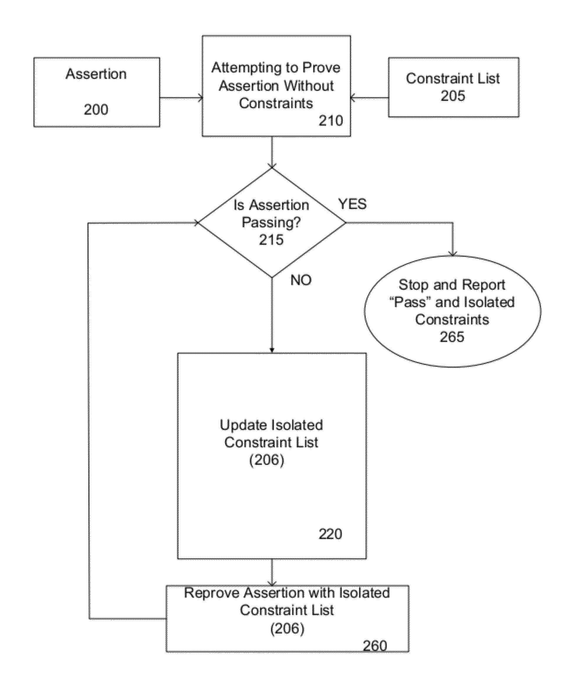
[0025]Reference will now be made in detail to the embodiments of the present disclosure, examples of which are illustrated in the accompanying drawings. The present disclosure may, however, be embodied in many different forms and should not be construed as being limited to the embodiments set forth herein; rather, these embodiments are provided so that this disclosure will be thorough and complete, and will fully convey the concept of the present disclosure to those skilled in the art. In the drawings, the thicknesses of layers and regions may be exaggerated for clarity. Like reference numerals in the drawings denote like elements.
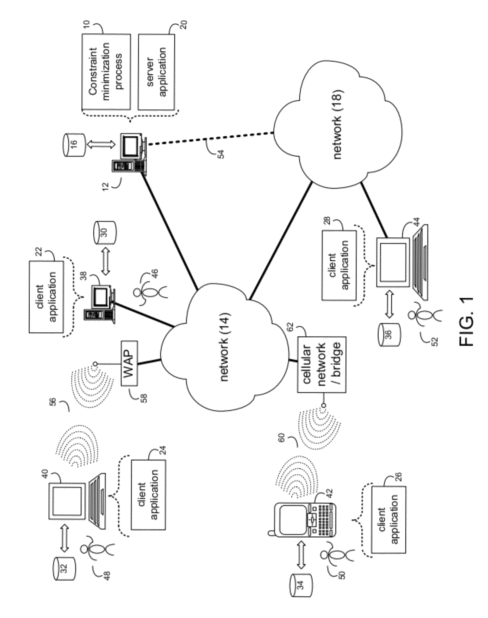
System Overview

[0026]Referring to FIG. 1, there is shown constraint minimization process 10 that may reside on and may be executed by server computer 12, which may be connected to network 14 (e.g., the internet or a local area network). Examples of server computer 12 may include, but are not limited to: a personal computer, a server computer, a series of s...


PUM


Abstract

The present disclosure relates to a method for minimizing constraints in the formal verification of an integrated circuit design. The method may include obtaining an unisolated list of constraints initially comprising all known constraints for the integrated circuit design and obtaining an isolated list of constraints initially comprising none of the known constraints. The method may further include attempting to prove an assertion without the known constraints and determining if the assertion is valid. The method may further include updating the isolated list of constraints.

Description

FIELD OF THE INVENTION[0001]The embodiments of the present disclosure relate to a method of formal verification, and more particularly, to a method of minimizing constraints during formal verification. Although embodiments of the present disclosure may be suitable for a wide scope of applications, one or more embodiments may be configured to reduce the number of constraints required for formal verification of a semiconductor design.BACKGROUND[0002]In general, it may be desirable to identify errors in semiconductor design while the semiconductor is in the design phase. As production moves from design to tooling and fabrication, the cost to fix design errors increases greatly. This great increase in cost may be attributable to specialized fabrication hardware that may have to be modified to repair a design error. A very small change in design can have cascading effects to other areas of the semiconductor. If these changes are made in while the semiconductor is in the design phase, sof...

Claims


Application Information

Patent Timeline
Patent Type & Authority Patents(United States)
IPC IPC(8): G06F17/50
CPCG06F17/504G06F30/3323
Inventor GOYAL, PRADEEPJAIN, ALOK
Owner CADENCE DESIGN SYST INC
Learn More