Thin film balun

a thin film balun and balun technology, applied in the field of balun, can solve the problem of inability to maintain the miniaturization of the balun, and achieve the effect of maintaining the miniaturization and improving the balance characteristics

Active Publication Date: 2012-11-27
TDK CORPARATION
View PDF10 Cites 6 Cited by
  • Summary
  • Abstract
  • Description
  • Claims
  • Application Information

AI Technical Summary

Benefits of technology

[0007]The present invention was conceived in view of the above-mentioned circumstances, and has an object of providing a thin film balun that can improve balance characteristics while maintaining miniaturization.
[0010]For example, the auxiliary coil portion is preferably connected between the fourth coil portion and the second balanced terminal. Moreover, the auxiliary coil portion is preferably positioned in at least one of an area facing coil conductors of the first and third coil portions and an area facing coil conductors of the second and fourth coil portions. As an example, the auxiliary coil portion is positioned in the area facing the coil conductors of the second and fourth coil portions. It has been verified by the inventors of the present application that these structures have effects of improving the balance characteristics of the thin film balun, though detailed actions are not clear.

Problems solved by technology

However, when a length of a coil is increased on a same plane to improve balance characteristics, a surface area of the coil increases, which makes it impossible to maintain the miniaturization of the balun.

Method used


Image

  • Thin film balun
  • Thin film balun
  • Thin film balun

Examples


example 1a

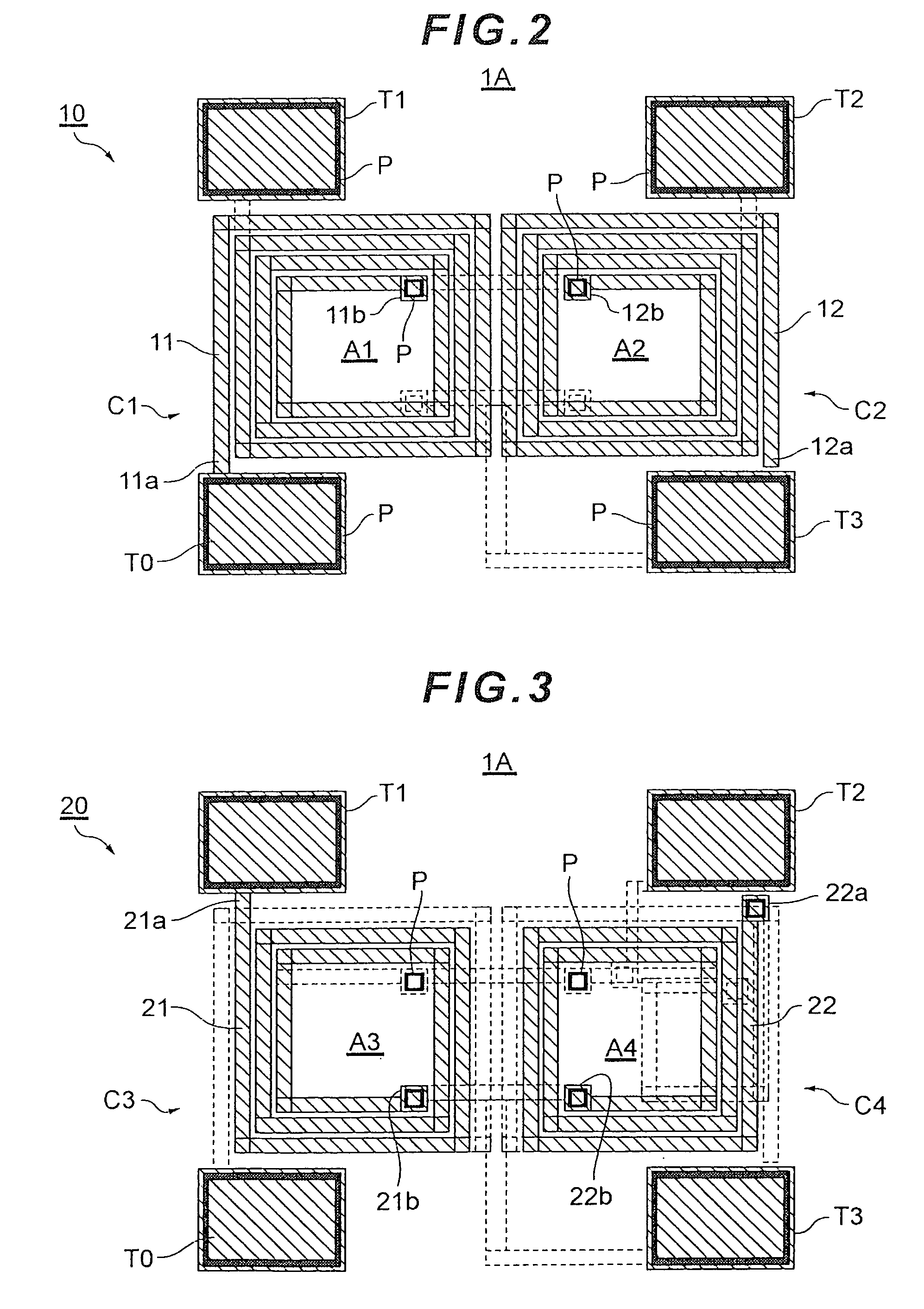
[0068]FIGS. 2 to 6 are plan views of individual wiring layers of a thin film balun 1A in an example 1A. In detail, FIG. 2 is a plan view of a first wiring layer 10, FIG. 3 is a plan view of a second wiring layer 20, FIG. 4 is a plan view of a third wiring layer 30, FIG. 5 is a plan view of a fourth wiring layer 40, and FIG. 6 is a plan view of a fifth wiring layer 50. The first wiring layer 10 is a lowermost wiring layer, and the fifth wiring layer 50 is an uppermost wiring layer. A substrate is located under the first wiring layer 10 which is the lowermost layer, though not shown in the drawings. That is, the thin film balun is formed on the substrate.

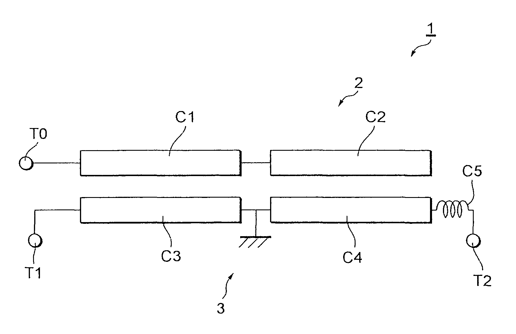
[0069]As shown in FIGS. 2 to 6, the unbalanced terminal T0, the first balanced terminal T1, the second balanced terminal T2, and a ground terminal T3 are formed on all layers of the first wiring layer 10 to the fifth wiring layer 50. Each of the terminals T0 to T3 is electrically connected between different layers via a through hole P...

example 1b

[0080]In an example 1B, the auxiliary coil portion C5 is positioned so as not to overlap the coil openings and the coil conductors of the first coil portion C1 and the second coil portion C2. FIGS. 7 and 8 are plan views respectively showing the fourth wiring layer 40 and the fifth wiring layer 50 of a thin film balun 1B in the example 1B. Note that the first wiring layer 10 to the third wiring layer 30 of the thin film balun 1B in the example 1B have the same structures as the example 1A.

[0081]As shown in FIGS. 7 and 8, the auxiliary coil portion C5 is constituted by a coil conductor 43 of the fourth wiring layer 40 and a coil conductor 52 of the fifth wiring layer 50. One end of the coil conductor 43 is connected to one end of the coil conductor 52 via a through hole P, and the other end of the coil conductor 43 is connected to the end 22a of the coil conductor 22 constituting the fourth coil portion C4 via a through hole P. The other end 52a of the coil conductor 52 is connected ...

example 1f

[0096]In the example 1F, the auxiliary coil portion C5 is formed by the third wiring layer 30 and the fourth wiring layer 40. FIGS. 16 and 17 are plan views respectively showing the third wiring layer 30 and the fourth wiring layer 40 of a thin film balun 1F in the example 1F. Note that the first wiring layer 10 and the second wiring layer 20 of the thin film balun 1F in the example 1F have the same structures as the example 1A. In addition, the fifth wiring layer 50 of the example 1A is unnecessary in the example 1F.

[0097]As shown in FIGS. 16 and 17, the auxiliary coil portion C5 is constituted by coil conductors 33, 34, and 48 of the third wiring layer 30 and the fourth wiring layer40. Connection relationships of the coil conductors 33, 34, and 48 are the same as the coil conductors 41, 42, and 51 in the example 1A.

[0098]In the example 1F, the auxiliary coil portion C5 is positioned in an area facing the coil conductors of the second coil portion C2 and the fourth coil portion C4 ...


PUM


Abstract

To provide a thin film balun that can improve balance characteristics while maintaining miniaturization. In a thin film balun to which an embodiment relates, an auxiliary coil portion is disposed at a predetermined position so as to face any one of an unbalanced transmission line and a balanced transmission line.

Description

BACKGROUND OF THE INVENTION[0001]1. Field of the Invention[0002]The present invention relates to a balun that performs conversion between unbalanced and balanced signals, and in particular relates to a thin film balun that is formed by a thin film process advantageous for smaller and thinner models.[0003]2. Description of the Related Art[0004]A wireless communication device includes various high frequency elements such as an antenna, a filter, an RF switch, a power amplifier, an RF-IC, and a balun. Of these elements, a resonant element such as an antenna or a filter handles an unbalanced signal which is based on a ground potential, whereas an RF-IC which generates or processes a high frequency signal handles a balanced signal. Accordingly, when connecting these two elements, a balun that functions as an unbalanced-balanced converter is used.[0005]In design of the above-mentioned balun, lengths and shapes of coils (line portions) are optimized so that desired balance characteristics ...

Claims


Application Information

Patent Timeline
Patent Type & Authority Patents(United States)
IPC IPC(8): H03H7/42H01P3/08
CPCH01F17/0013H01F27/2804H03H7/422H01P5/10H03H2001/0078
Inventor ENDO, MAKOTO
Owner TDK CORPARATION
Why Eureka
Try Eureka