Wiring board and liquid crystal display device

a liquid crystal display device and wiring board technology, applied in the direction of instruments, sustainable manufacturing/processing, semiconductor/solid-state device details, etc., can solve problems such as leakage failure and leakage failur

Active Publication Date: 2012-11-27
SHARP KK
View PDF20 Cites 0 Cited by
  • Summary
  • Abstract
  • Description
  • Claims
  • Application Information

AI Technical Summary

Benefits of technology

[0025]In this arrangement, the pad 109 is disposed away from the metal wire 101. This prevents the occurrence of a leak failure in the region RS1.
[0063]This allows for production of a wiring board and a liquid crystal display device, each of which has a reduced risk of a leak failure and achieves a narrower pad pitch.

Problems solved by technology

The arrangement of Patent Literature 1 unfortunately tends to cause a problem of a leak failure between a pad 109 and a metal wire 101 when an electronic component such as a driving IC is mounted.
As described above, a leak failure occurs in the case where a corner portion of a connecting line formed between pads adjacent to each other comes into contact with one of the pads.

Method used


Image

  • Wiring board and liquid crystal display device
  • Wiring board and liquid crystal display device
  • Wiring board and liquid crystal display device

Examples


embodiment

[0110](Present Embodiment)

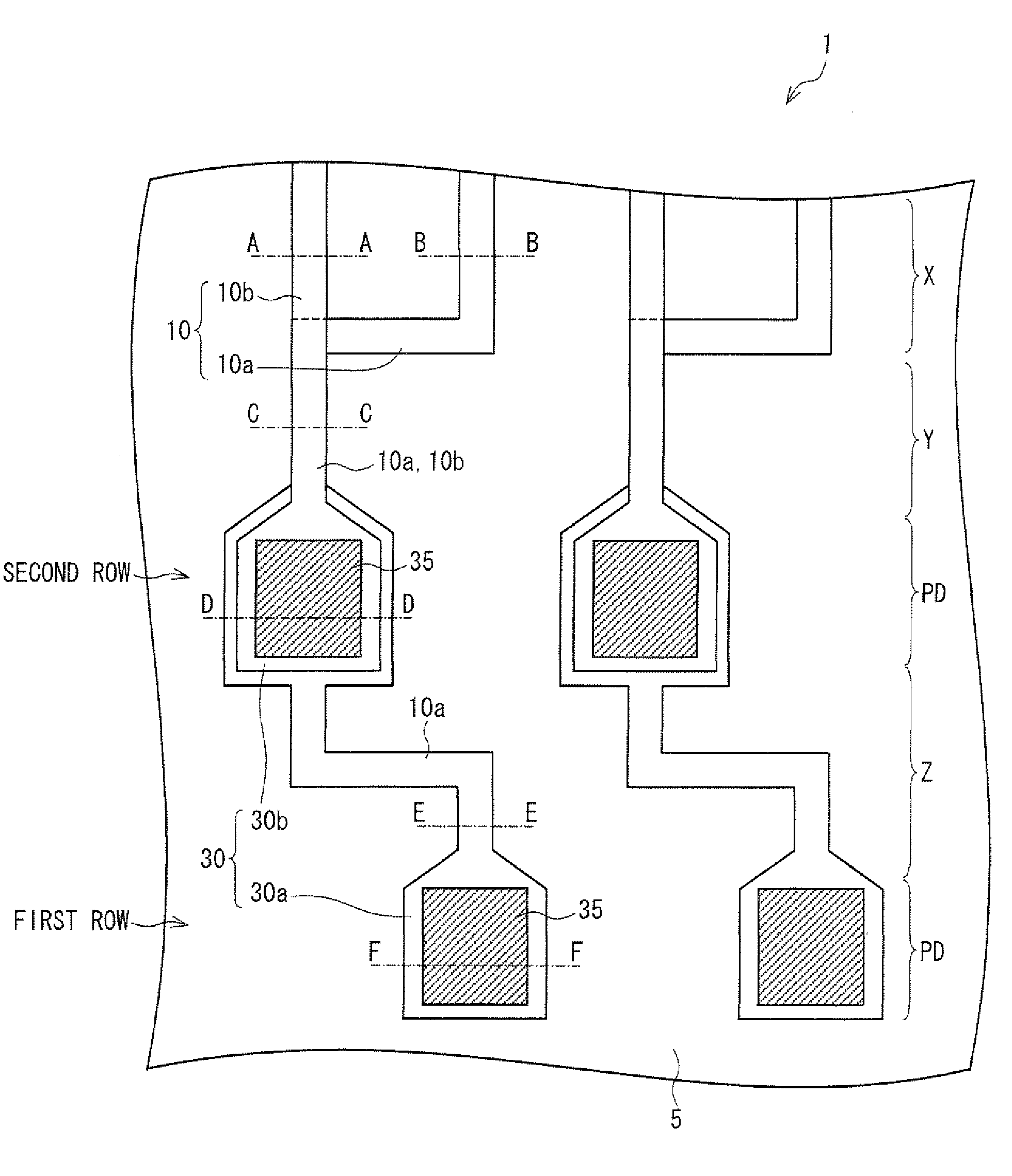
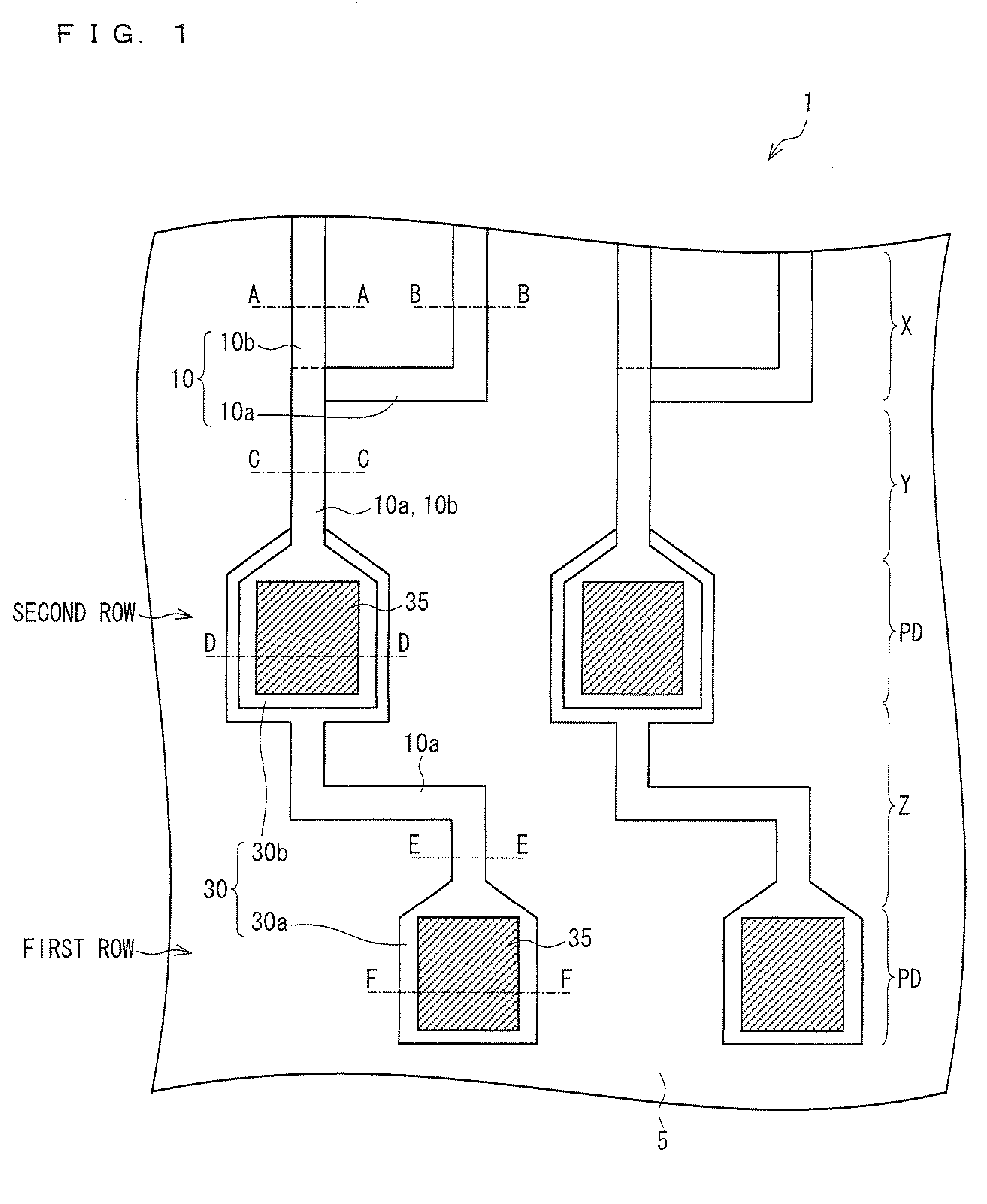
[0111]In contrast, according to the wiring board 1 of the present embodiment, while first metal wires 10a each connected to a first-row pad 30a and second metal wires 10b each connected to a second-row pad 30b are provided in a single layer on the substrate 5 in a drawing region (region X illustrated in FIG. 1), the first and second metal wires 10a and 10b are provided in separate layers in a second connection region (region Y illustrated in FIG. 1), in which the second metal wires 10b are connected to the corresponding second-row pads 30b.

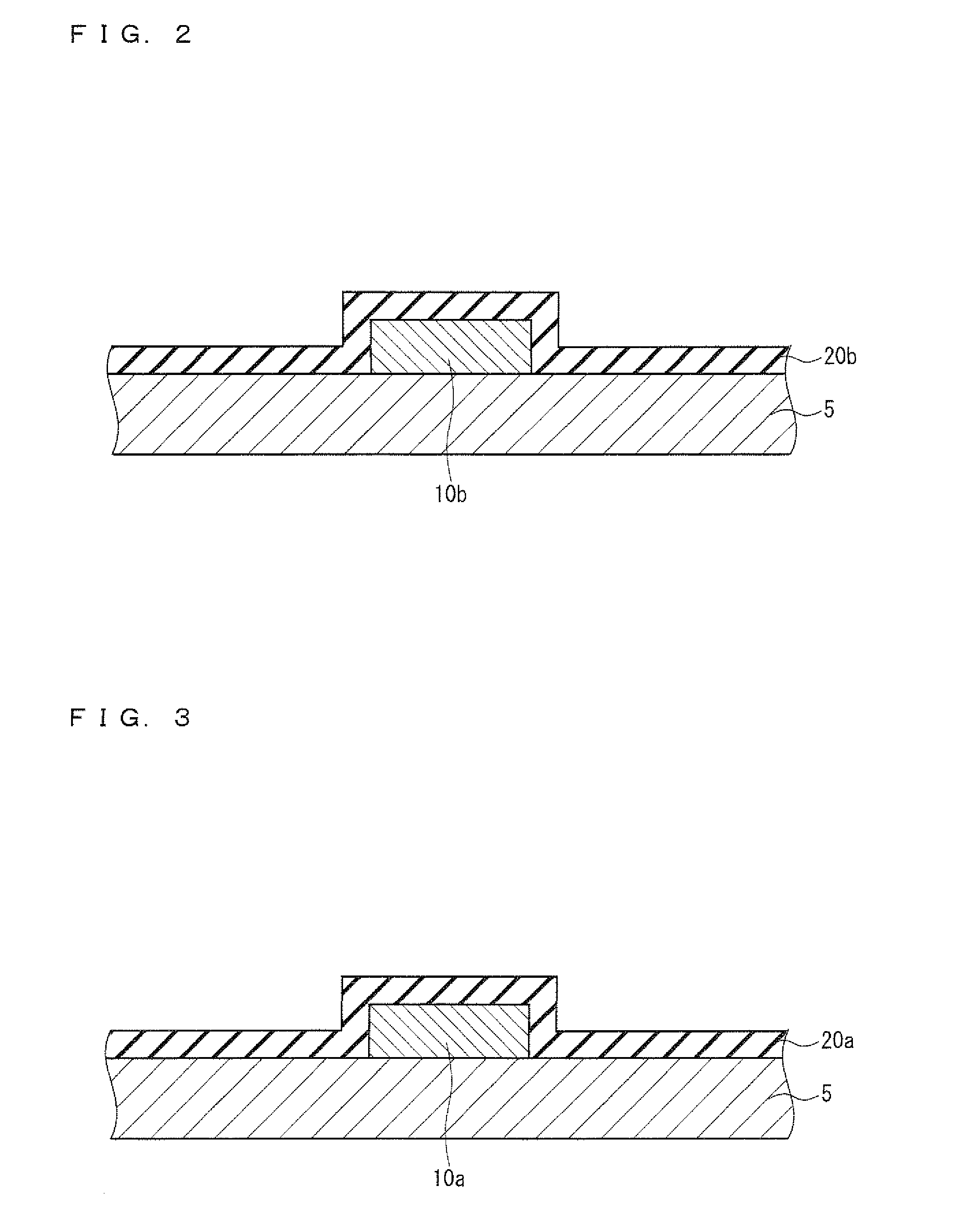
[0112]More specifically, as illustrated in FIGS. 2 and 3, the first and second metal wires 10a and 10b are, although made of different materials as described below, provided in a single layer on the substrate 5 in the drawing region X. Further, the first and second metal wires 10a and 10b are covered with first and second insulating layers 20a and 20b, respectively.

[0113]FIG. 2 is a cross-sectional view (taken along line...

case 1

[0160](Leak Failure: Case 1)

[0161]The above arrangement, however, may cause a leak failure due to, e.g., sinking of a second-row pad 30b. This is described below.

[0162]As described above, electronic components such as a driving IC are mounted to the second-row pads 30b. Specifically, each bump 120 of an electronic component is, for example, joined, by compression in a direction indicated by an arrow shown in FIG. 13, to a second-row pad 30b (more specifically, to a pad electrode 32 formed on the second-row pad 30b). This causes a current to flow between the electronic component and the second-row pads 30b.

[0163]The electronic component may be mounted with a great force (indicated by the arrow shown in FIG. 13) that is applied from each bump 120 of the electronic component to a corresponding second-row pad 30b so as to press the second-row pad 30b toward the substrate 5. In this case, the above force may deform the second-row pad 30b.

[0164]The following description refers to FIG. 1...


PUM

PropertyMeasurementUnit
lengthaaaaaaaaaa
widthaaaaaaaaaa
sizeaaaaaaaaaa

Abstract

A wiring board of the present invention (1) is arranged so that: pads (30) arranged in a plurality of rows include: first-row pads (30a) connected to first metal wires (10a) among metal wires (10); and second-row pads (30b) connected to second metal wires (10b) among the metal wires (10), the first metal wires (10a) being longer than the second metal wires (10b); each of the first metal wires (10a) is formed so as to be separated from a corresponding one of the second-row pads (30b) by at least an insulating layer, and so as to have a widthwise center in a lower region below the corresponding second-row pad (30b); and each of the first metal wires (10a) has widthwise edges provided, in a plan view, beyond widthwise edges of a corresponding one of the second-row pads (30b) in a region in which the first metal wire (10a) overlaps with the corresponding second-row pad (30b).

Description

[0001]This application is the U.S. national phase of International Application No. PCT / JP2008 / 062956, filed 17 Jul. 2008, which designated the U.S. and claims priority to Japanese Patent Application No. 2007-210344, filed Aug. 10, 2007, the entire contents of each of which are hereby incorporated by reference.TECHNICAL FIELD[0002]The present invention relates to a wiring board. In particular, the present invention relates to a wiring board having pads arranged in a plurality of rows and to a liquid crystal display device including such a wiring board.BACKGROUND ART[0003]Conventionally, there has been widely used a wiring board having pads arranged in a so-called plurality of rows for a narrow-pitch mounting.[0004]In view of a demand for further reduction in size and weight of electronic devices including the wiring board, electronic components in each of such electronic devices are mounted at a higher density. Accordingly, the wiring board on which the electronic components are moun...

Claims


Application Information

Patent Timeline
Patent Type & Authority Patents(United States)
IPC IPC(8): G02F1/1345
CPCG02F1/1345H05K1/111H05K1/117G02F1/13458Y02P70/611G02F2001/13629H01L2924/01013H01L2924/01022H01L2924/01033H01L2924/01046H01L2924/01049H01L2924/01073H01L2924/01082H01L2924/04941H01L2924/04953H01L2924/14H05K3/4644H05K2201/09672H05K2201/09709H01L2924/01005H01L2924/01006H01L2924/01019H01L2224/17155H01L2224/16227H01L2924/00013H01L2224/16225H01L2224/13099H01L2224/13599H01L2224/05599H01L2224/05099H01L2224/29099H01L2224/29599Y02P70/50G02F1/13629
Inventor MATSUI, TAKASHISHIOTA, MOTOJI
Owner SHARP KK
Why Eureka
Try Eureka