Optical signal processing device

a signal processing and optical signal technology, applied in optical multiplex, wavelength-division multiplex systems, instruments, etc., can solve the problems of temperature dependence in signal processing characteristics, deterioration of optical signal processing devices, fluctuation of position, etc., and achieve accurate temperature compensation and simple and low-cost methods.

Active Publication Date: 2013-01-01
NIPPON TELEGRAPH & TELEPHONE CORP
View PDF8 Cites 15 Cited by
  • Summary
  • Abstract
  • Description
  • Claims
  • Application Information

AI Technical Summary

Benefits of technology

[0013]Conventionally, in order to solve the temperature dependency of the spectroscopic characteristics of AWG, an approach has been considered to reduce the temperature dependency of the spectroscopic characteristics of AWG itself. For example, Patent Publication 2 discloses a technique to perform temperature compensation by a configuration where an array waveguide of AWG include a plurality of characteristic grooves dividing a core. However, this technique cannot avoid an excess loss of about 1 dB even when the grooves have an optimal shape so that the loss can be minimized. Furthermore, the formation of the groove structure requires an addition of a complicated step to the manufacture of AWG, thus causing a disadvantage of a high manufacture cost.
[0014]A disadvantage caused by the temperature dependency of the spectroscopic characteristics of AWG also may cause a disadvantage in an optical signal processing device not including a focusing lens. As described above, it has been required to solve, in a simple and low-cost manner, the disadvantage of the temperature dependency of the performance of an optical signal processing device caused by the temperature dependency of the spectroscopic characteristics owned by AWG.
[0024]As described above, according to the present invention, a temperature fluctuation in the performance of the optical signal processing device caused by the temperature dependency of the spectroscopic characteristics owned by the spectroscopic means can be suppressed, in a simpler and low-cost method, by directly controlling the modulation characteristic profile formed based on a configuration unit of the spatial light modulator. Furthermore, more accurate temperature compensation also can be provided in accordance with the real behavior of the device to a temperature fluctuation including causing factors of a complicated temperature fluctuation in the entire optical system. The same effect also can be expected also in the case where AWG is used as the spectroscopic means.

Problems solved by technology

However, in a conventional optical signal processing device, a disadvantage has been caused in which the temperature dependency of the spectroscopic characteristics of the spectroscopic element causes a temperature change which causes a deteriorated performance of the optical signal processing device.
Even in the case of optical signals having the same wavelength, a temperature change causes a change in the outgoing angle thereof, which causes a fluctuation of the position of the focusing point on the signal processing device.
This consequently causes a temperature dependency in the signal processing characteristic (e.g., light loss) and a phase shift given to an optical signal.
However, this technique cannot avoid an excess loss of about 1 dB even when the grooves have an optimal shape so that the loss can be minimized.
Furthermore, the formation of the groove structure requires an addition of a complicated step to the manufacture of AWG, thus causing a disadvantage of a high manufacture cost.
A disadvantage caused by the temperature dependency of the spectroscopic characteristics of AWG also may cause a disadvantage in an optical signal processing device not including a focusing lens.
As described above, it has been required to solve, in a simple and low-cost manner, the disadvantage of the temperature dependency of the performance of an optical signal processing device caused by the temperature dependency of the spectroscopic characteristics owned by AWG.

Method used


Image

  • Optical signal processing device
  • Optical signal processing device
  • Optical signal processing device

Examples


embodiment 1

Illustrative Embodiment 1

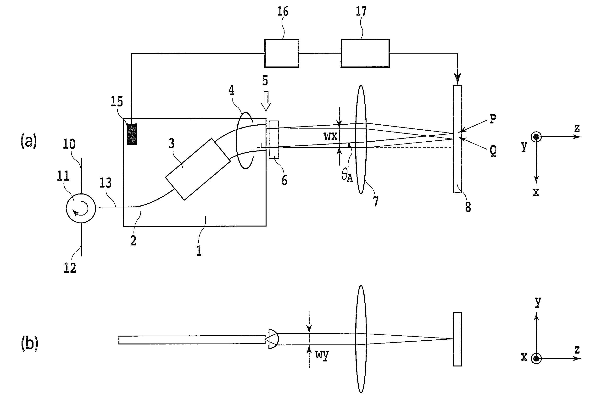
[0033]FIGS. 1(a) and 1(b) illustrate the configuration of an optical signal processing device according to the illustrative embodiment 1 of the present invention. The present invention can be applied to an optical signal processing device that includes a spatial phase control device having a plurality of element devices as a signal processing device. FIG. 1(a) is a top view. FIG. 1(b) is a side view. In the illustrative embodiment 1, the operation will be described by way of a dispersion compensator in which the feature of the present invention can be achieved at the maximum. With reference to FIG. 1(a), the dispersion compensator according to the present invention is composed of: a circulator 11 for inputting and outputting an optical signal; an Arrayed Waveguide Grating 1 (hereinafter referred to as AWG) configuring spatial optical system; a cylindrical lens 6; a focusing lens 7; and a spatial phase control device 8. An inputted optical signal is reflected...

embodiment 2

Illustrative Embodiment 2

[0063]The dispersion compensator of FIG. 1 that has been described heretofore has a configuration in which a focusing lens is included in the spatial optical system and an optical signal is focused on the spatial phase control device. In this case, the beam diameter on the spatial phase control device as an optical coupling plane may be larger than the pixel repetition cycle of the element device. The present invention also can be applied to an optical signal processing device not including a focusing lens such as a tunable wavelength filter. Even in the case of the optical signal processing device having a configuration not including a focusing lens, it is possible to compensate the temperature dependency of the spectroscopic characteristics of a spectroscopic element such as AWG. Next, the following section will describe an example of an optical signal processing device that uses a spatial phase control device as a signal processing device and that has a f...


PUM

PropertyMeasurementUnit
refractive index ngaaaaaaaaaa
focal lengthaaaaaaaaaa

Abstract

A conventional optical signal processing device had a disadvantage where the temperature dependency of the spectroscopic characteristics of a spectroscopic element causes a deteriorated performance. In order to solve the temperature dependency, there has been a method to form a plurality of grooves for dividing a core on the array waveguide of the AWG. However, this method cannot avoid an excess loss and causes a high manufacture cost. By directly controlling the modulation characteristic profile formed by an element device of a spatial light modulator, athermalization can be achieved in a simpler and low-cost manner. This consequently provides a remarkable reduction of the light coupling loss in the spatial optical system of the optical signal processing device. More accurate temperature compensation can be realized that copes with an actual behavior of the device to a temperature fluctuation, including causing factors of a complicated temperature fluctuation of the optical system.

Description

TECHNICAL FIELD[0001]The present invention relates to an optical signal processing device. More particularly, the present invention relates to the temperature compensation of the optical signal processing device including a spectroscopic means.BACKGROUND ART[0002]With more optical communication networks having a higher speed and a higher capacity, increasing demands have been placed on optical signal processing devices for performing the processing of Wavelength Division Multiplexing (WDM) optical signals. For example, a multiplexed optical signal at a node is not subjected to an optical to electrical conversion but the optical signal is directly subjected to a path switching. Thus, transparent optical signal processing devices have been promoted.[0003]On the other hand, from the viewpoint of the downsizing and integration of an optical signal processing device, Planar Lightwave Circuits (PLC) have been researched and developed. The PLC is structured so that a silicon substrate for ...

Claims


Application Information

Patent Timeline
Patent Type & Authority Patents(United States)
IPC IPC(8): H04J14/02G02B27/00G02F1/01G02F1/03G02F1/061G02F1/13
CPCG02B6/12019G02B6/12026G02F1/0121G02F1/13306G02F1/136277G02F2203/12G02F2203/60
Inventor SUZUKI, KENYAOOBA, NAOKIISHII, MOTOHAYAMINO, SHINJISENO, KAZUNORI
Owner NIPPON TELEGRAPH & TELEPHONE CORP
Why Eureka
Try Eureka