
Field-effect transistor

a field-effect transistor and transistor technology, applied in the direction of basic electric elements, electrical apparatus, semiconductor devices, etc., can solve the problems of substrate becoming less resistive at higher temperatures, difficult substrate for gan epitaxial growth, so as to reduce parasitic capacitance effectively with the substrate, prevent the rise in the channel temperature, and reduce the effect of thermal resistivity

Active Publication Date: 2013-08-13
MITSUBISHI ELECTRIC CORP
View PDF6 Cites 17 Cited by
  • Summary
  • Abstract
  • Description
  • Claims
  • Application Information

AI Technical Summary

Benefits of technology

The invention provides a FET that prevents the rise in channel temperature between neighboring FETs on a substrate by increasing the gate pitch. By dividing the drain electrode into multiple smaller sub-electrodes and insulating the drain ohmic contacts from each other, the area of the drain electrode and the conductive layer under it are reduced, resulting in decreased parasitic capacitance with the substrate and reduced temperature dependence of drain efficiency. This allows for more efficient operation at high temperatures. Additionally, the invention allows for the use of a low-cost Si substrate in GaN wafer production, reducing costs.

Problems solved by technology

GaN substrate for GaN epitaxial growth is difficult to make.
However, Si does not provide a semi-insulating property (1.0×10⁶ Ωcm or more in resistivity) and only Si substrates with a resistivity of 1.0×10⁶ Ωcm or less are available.
Therefore, as shown in FIG. 8, Si has a temperature dependence of its resistivity, posing a problem that the substrate becomes less resistive at higher temperatures.
However, a low-resistivity Si substrate would generate a parasitic capacitance even at room temperature, leading to a lower efficiency.
For this reason, as far as an existing GaN-on-Si wafer is used, the high temperature operation, which is inherent property in GaN as a wide band gap semiconductor, cannot be sufficiently achieved.
Hei 5 (1993)-190574, the drain electrode area is decreased to some extent, but generation of a parasitic capacitance in the lattice-shaped drain electrode cannot be avoided and the efficiency improvement is limited.
Particularly, in the case of a GaN-FET which generates a high concentration of two-dimensional electron gas, the influence of the parasitic capacitance between the channel under the drain electrode and the substrate is significant and it seems that a sufficient improvement cannot be achieved simply by decreasing the drain electrode area.
But actually a local rise in the channel temperature cannot be avoided because the channel temperature of two neighboring FETs with a narrow drain electrode between them would be much higher than the average channel temperature of the whole device.

Method used


Image

  • Field-effect transistor
  • Field-effect transistor
  • Field-effect transistor

Examples


first embodiment

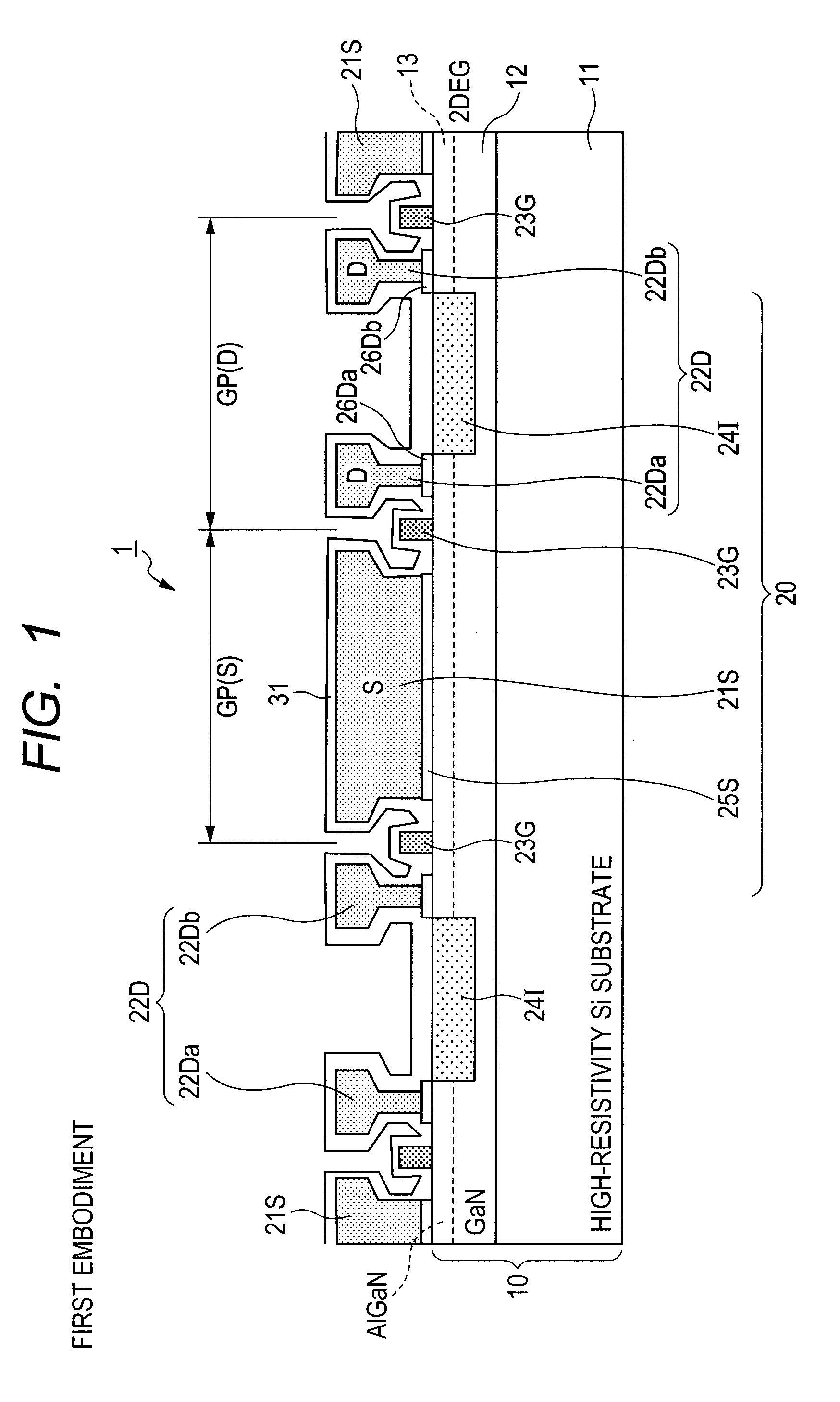
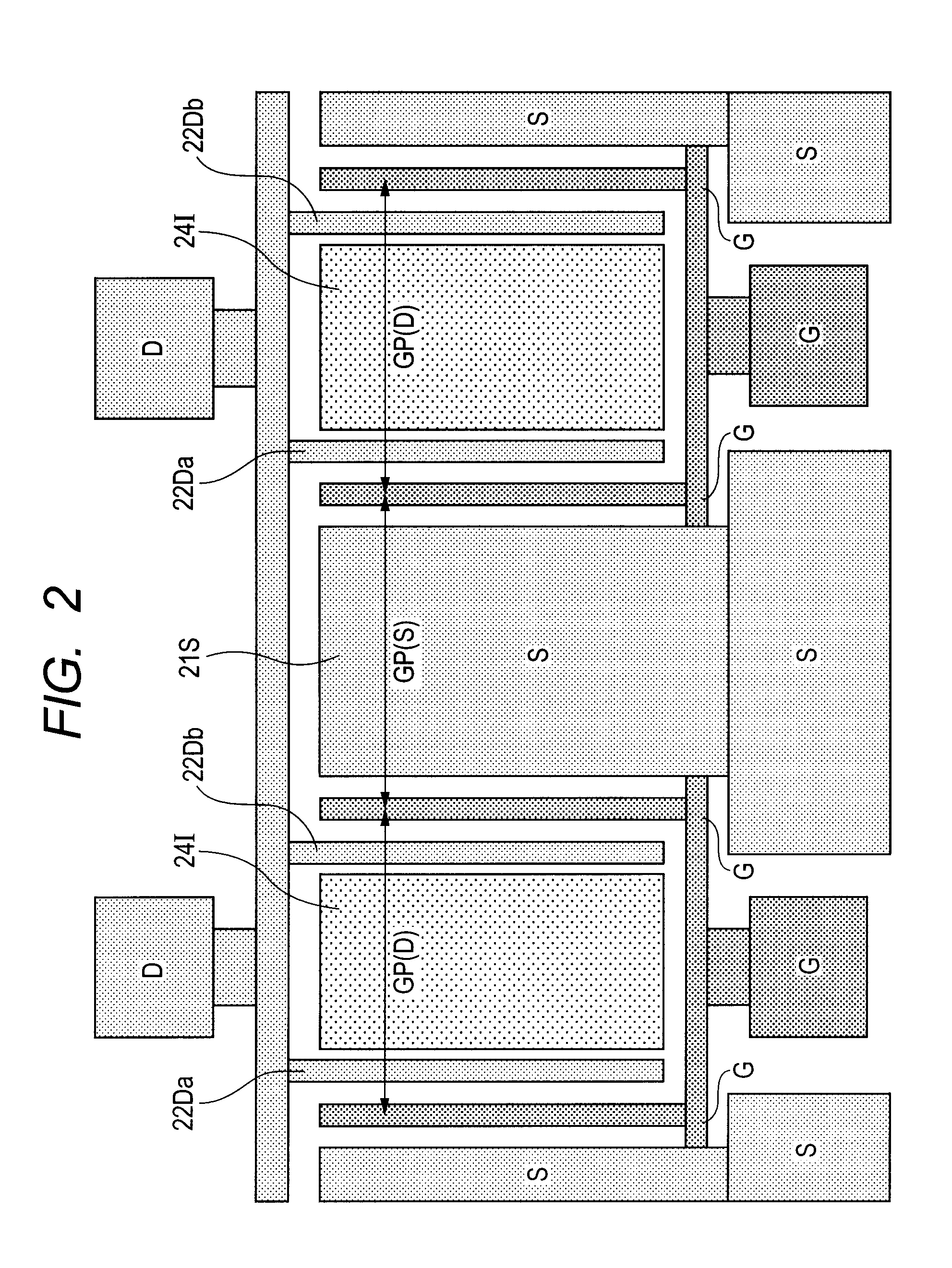
[0053]Next, the structure of a semiconductor device with a field-effect transistor (FET) according to a first embodiment of the present invention will be described referring to the accompanying drawings. FIG. 1 is a schematic sectional view of the semiconductor device according to this embodiment and FIG. 2 is a plan view of an essential part of the device. For easy understanding, the scales and positions of the elements shown in the figures are different from their actual scales and positions. In the sectional view, hatching is omitted as appropriate.

[0054]As shown in FIGS. 1 and 2, the semiconductor device 1 according to this embodiment is structured as follows: a plurality of FETs 20, each FET having a source electrode 21S, a drain electrode 22D, and a gate electrode 23G, are formed on a GaN epitaxial wafer 10 in which a GaN epitaxial layer 12 has grown over a high-resistivity Si substrate 11 with a resistivity value of 1.0×10² Ωcm or more and an AlGaN layer 13 has grown on it.

[0...

second embodiment

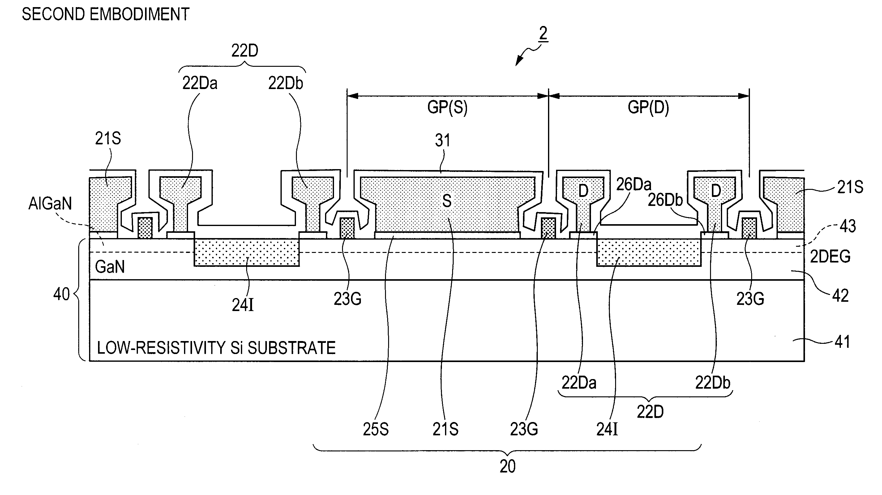
[0085]Next, the structure of a semiconductor device 2 according to a second embodiment of the present invention will be described referring to the accompanying drawings. FIG. 5 is a schematic sectional view of the semiconductor device with an FET according to the second embodiment. For easy understanding, the scales and positions of the elements shown in the figures are different from their actual scales and positions. The same elements as in the first embodiment are designated by the same reference numerals and their descriptions are omitted.

[0086]As shown in FIG. 5, the semiconductor device 2 according to the second embodiment is structured as follows: a plurality of FETs 20, each FET having a source electrode 21S, a drain electrode 22D, and a gate electrode 23G, are formed on a GaN epitaxial wafer 40 in which a GaN epitaxial layer 42 has grown on a low-resistivity Si substrate 41 with a resistivity of 1.0×10⁻¹ Ωcm or less and an AlGaN layer 43 has grown on it.

[0087]In this embodi...


PUM


Abstract

A field-effect transistor (FET) in which a gate electrode is located between a source electrode formed on one side of the gate electrode and a drain electrode formed on the other side, a source ohmic contact is formed under the source electrode and a drain ohmic contact is formed under the drain electrode. In the FET, the rise in the channel temperature is suppressed, the parasitic capacitance with a substrate is decreased, and the temperature dependence of drain efficiency is reduced, so that highly efficient operation can be achieved at high temperatures. The drain electrode is divided into a plurality of drain sub-electrodes spaced from each other and an insulating region is formed between the drain ohmic contacts formed under the drain sub-electrodes.

Description

CROSS-REFERENCE TO RELATED APPLICATIONS[0001]The disclosure of Japanese Patent Application No. 2010-72295 filed on Mar. 26, 2010 including the specification, drawings and abstract is incorporated herein by reference in its entirety.BACKGROUND[0002]1. Field of the Invention[0003]The present invention relates to field-effect transistors.[0004]2. Description of Related Art[0005]Field-effect transistors (hereafter referred to “FETs”) with higher power and higher efficiency are demanded for the amplifiers used in the cellular base-stations, with the advance of telecommunication technology.[0006]To date, Si-MOSFET (Metal-Oxide-Semiconductor FET), GaAs-MESFET (Metal-Semiconductor FET), and GaAs-HJFET (Hetero-Junction FET) have been used as the conventional Power FETs. HJFET is also referred to as HEMT (High Electron Mobility Transistor).[0007]In recent years, “GaN-FET”, which uses a wide band gap semiconductor GaN realizing high temperature operation, has been proposed as a high power FET....

Claims


Application Information

Patent Timeline
Patent Type & Authority Patents(United States)
IPC IPC(8): H01L29/15
CPCH01L21/823481H01L29/0692H01L29/41758H01L29/812H01L29/66856H01L29/66871H01L29/7787H01L29/66462H01L29/2003
Inventor ISHIKURA, KOHJI
Owner MITSUBISHI ELECTRIC CORP
Learn More