

Field-effect transistor
a field-effect transistor and transistor technology, applied in the direction of basic electric elements, electrical apparatus, semiconductor devices, etc., can solve the problems of substrate becoming less resistive at higher temperatures, difficult substrate for gan epitaxial growth, so as to reduce parasitic capacitance effectively with the substrate, prevent the rise in the channel temperature, and reduce the effect of thermal resistivity
- Summary
- Abstract
- Description
- Claims
- Application Information
AI Technical Summary
Benefits of technology
Problems solved by technology
Method used
Image

Examples
first embodiment
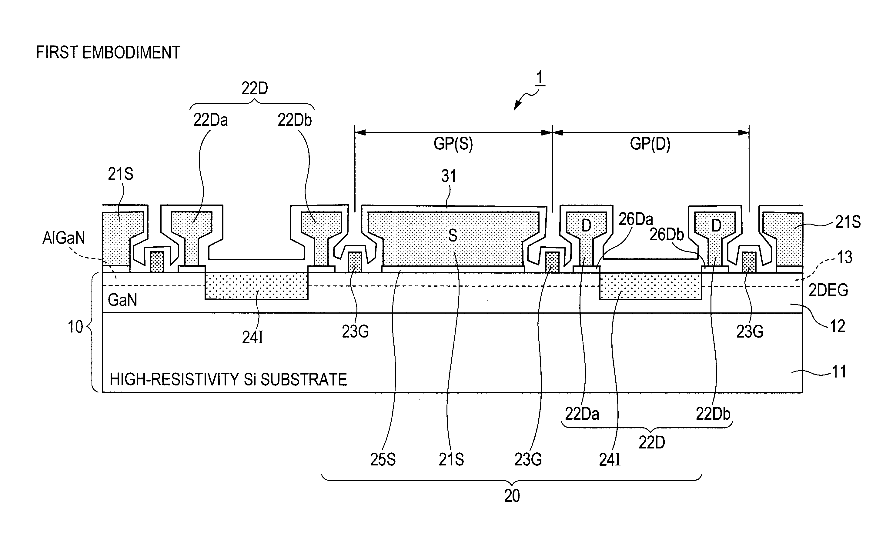
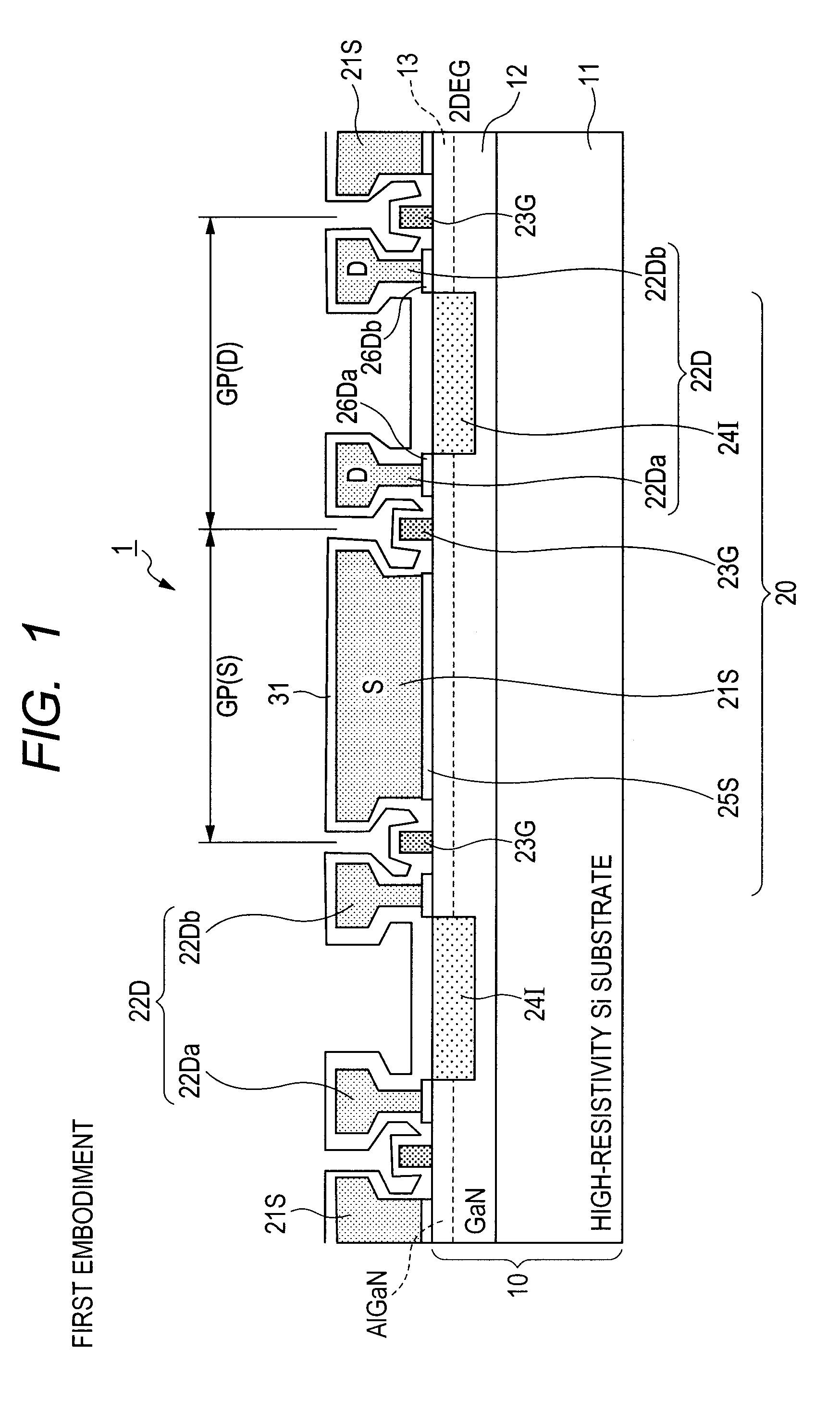
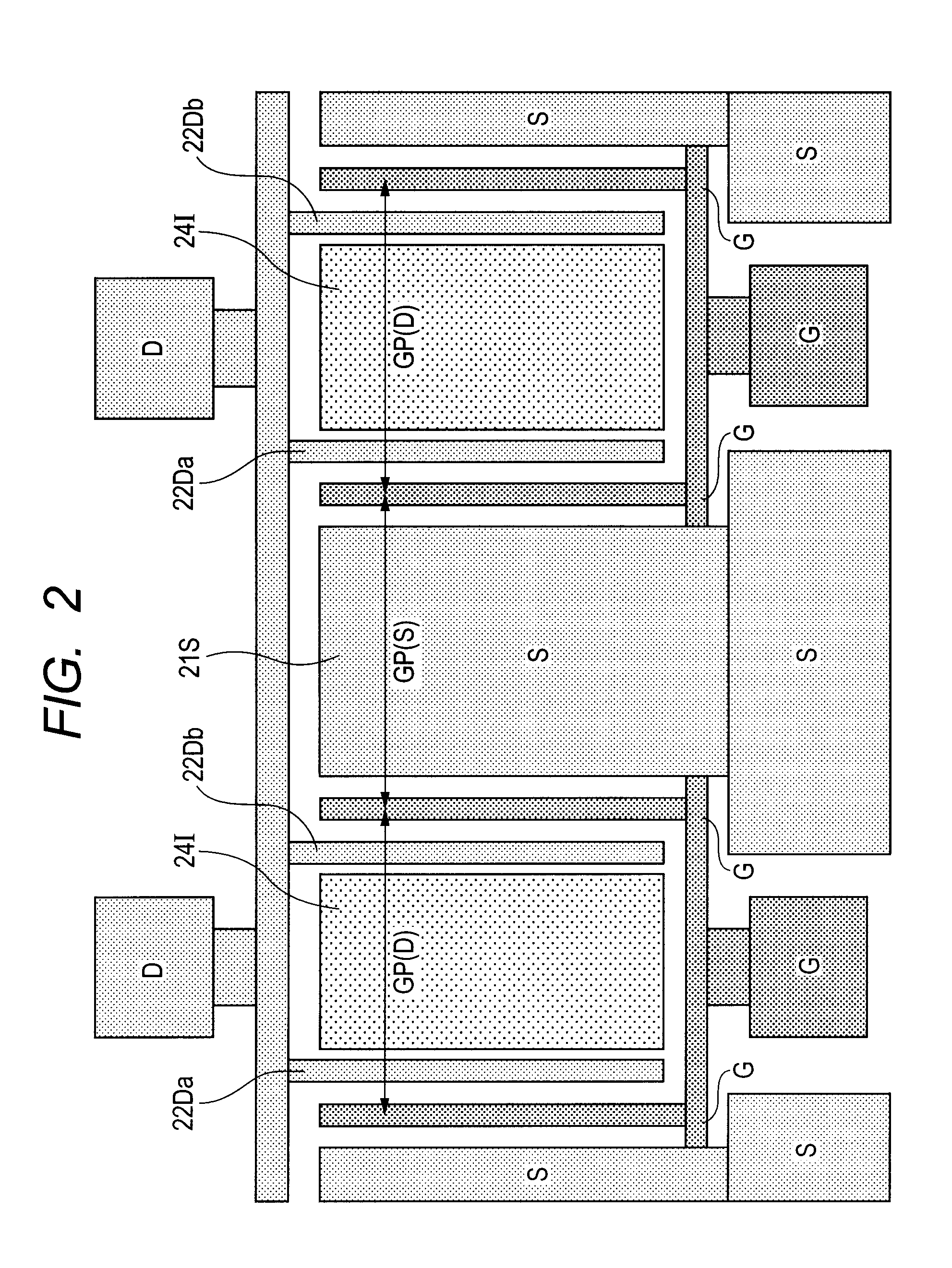
[0053]Next, the structure of a semiconductor device with a field-effect transistor (FET) according to a first embodiment of the present invention will be described referring to the accompanying drawings. FIG. 1 is a schematic sectional view of the semiconductor device according to this embodiment and FIG. 2 is a plan view of an essential part of the device. For easy understanding, the scales and positions of the elements shown in the figures are different from their actual scales and positions. In the sectional view, hatching is omitted as appropriate.
[0054]As shown in FIGS. 1 and 2, the semiconductor device 1 according to this embodiment is structured as follows: a plurality of FETs 20, each FET having a source electrode 21S, a drain electrode 22D, and a gate electrode 23G, are formed on a GaN epitaxial wafer 10 in which a GaN epitaxial layer 12 has grown over a high-resistivity Si substrate 11 with a resistivity value of 1.0×10² Ωcm or more and an AlGaN layer 13 has grown on it.
[0...
second embodiment
[0085]Next, the structure of a semiconductor device 2 according to a second embodiment of the present invention will be described referring to the accompanying drawings. FIG. 5 is a schematic sectional view of the semiconductor device with an FET according to the second embodiment. For easy understanding, the scales and positions of the elements shown in the figures are different from their actual scales and positions. The same elements as in the first embodiment are designated by the same reference numerals and their descriptions are omitted.
[0086]As shown in FIG. 5, the semiconductor device 2 according to the second embodiment is structured as follows: a plurality of FETs 20, each FET having a source electrode 21S, a drain electrode 22D, and a gate electrode 23G, are formed on a GaN epitaxial wafer 40 in which a GaN epitaxial layer 42 has grown on a low-resistivity Si substrate 41 with a resistivity of 1.0×10⁻¹ Ωcm or less and an AlGaN layer 43 has grown on it.
[0087]In this embodi...
PUM
 Abstract
Description
Claims
Application Information