Display device and electronic apparatus
a technology of electronic equipment and display device, applied in the field of display device and electronic equipment, can solve the problems of affecting touch detection, propagating to the touch panel, and generating various noises on the display panel, and achieve the effect of hardly susceptible to nois
- Summary
- Abstract
- Description
- Claims
- Application Information
AI Technical Summary
Benefits of technology
Problems solved by technology
Method used
Image

Examples
first embodiment
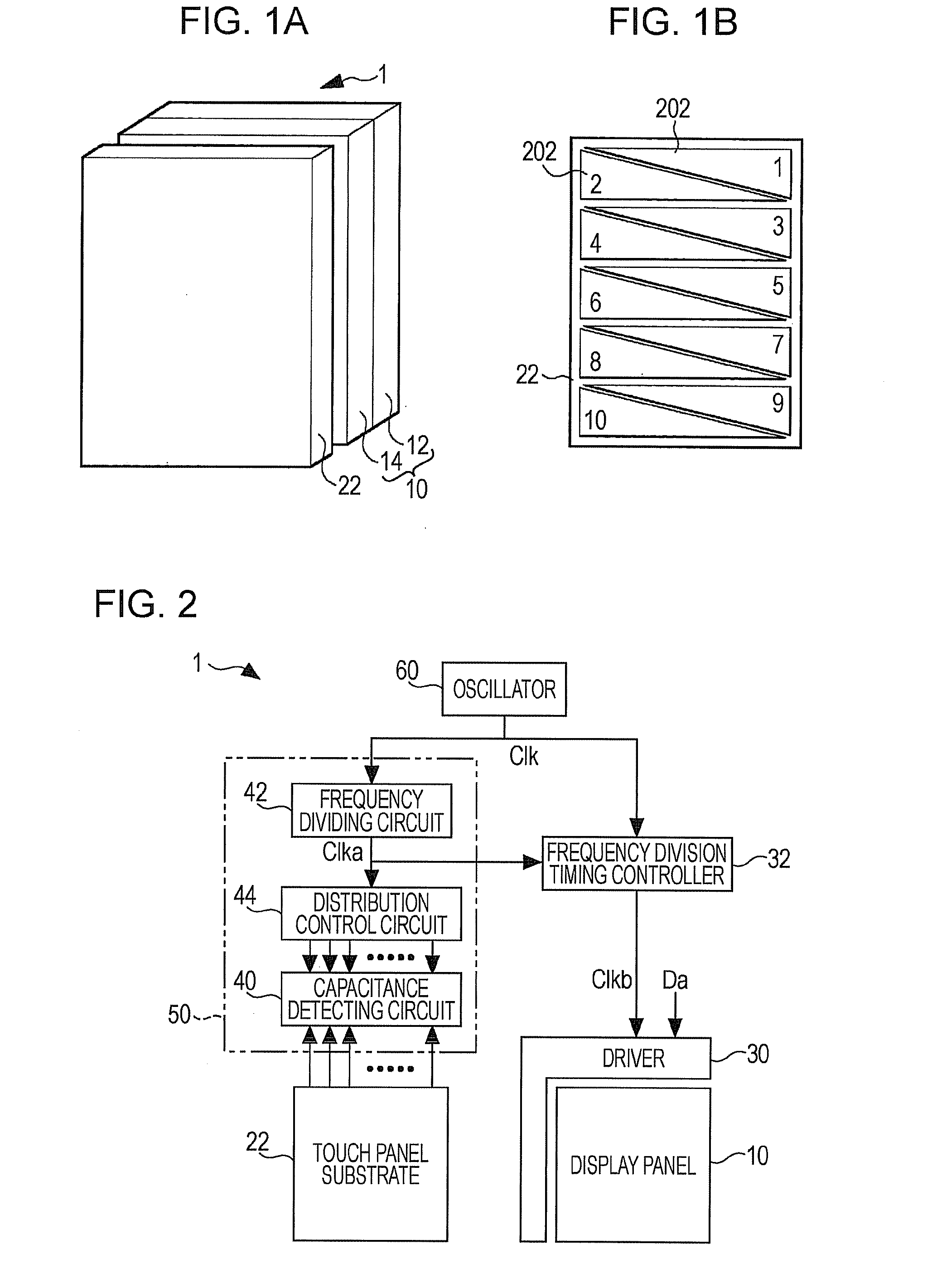
[0025]FIG. 1A illustrates the structure of a display device according to the invention.
[0026]Referring to FIG. 1A, the display device, indicated at 1, has a laminated structure including a display panel 10 and a touch panel substrate 22 having detection electrodes for touch detection. The display panel 10 includes an element substrate 12 and an opposite substrate 14 which are attached to each other with a predetermined space therebetween, and further includes a liquid crystal layer disposed in the space between those substrates. In FIG. 1A, the display panel 10 is separated from the touch panel substrate 22 for the convenience of explanation. Actually, the display panel 10 is in tight contact with the touch panel substrate 22.
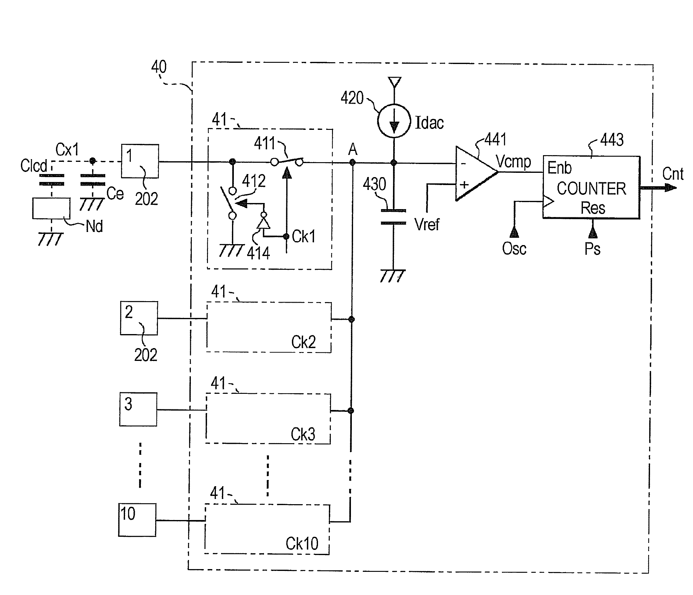
[0027]The touch panel substrate 22 has a plurality of (in the present embodiment, ten) detection electrodes 202 composed of a transparent conducting layer, as shown in FIG. 1B. In this embodiment, the detection electrodes 202 each having a right-angled triangul...
second embodiment
[0090] a signal Clka is not obtained by frequency division as shown in FIG. 1 but is generated from an oscillator 62. The oscillator 62, a capacitance detecting circuit 40, and a distribution control circuit 44 constitute a detector 50 in single-chip integrated form.
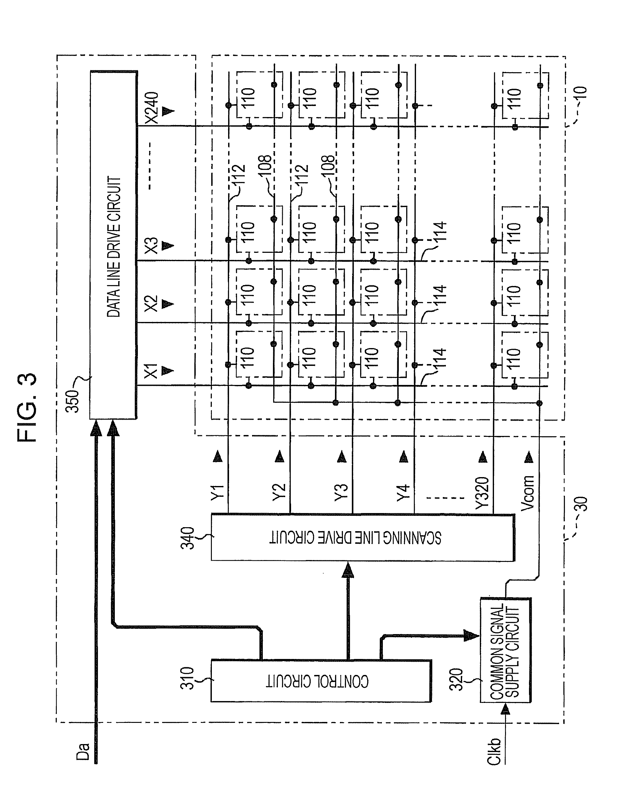
[0091]In the second embodiment, a frequency division timing controller 32 divides the frequency of an input signal by 38 in a manner similar to the first embodiment. The signal Clka, serving as an input signal, has a frequency that is ¼ the frequency of the clock signal Clk in the first embodiment. In the second embodiment, therefore, a common signal supply circuit 320 in a driver 30 may change a voltage of a common signal Vcom every horizontal scanning period (H) equivalent to a period corresponding to four pulses of a clock signal Clkb, which is obtained by dividing the frequency of the signal Clka by 38.
[0092]A third embodiment of the present invention will now be described. FIG. 11 is a block diagram illustrating the...
third embodiment
[0093]In the third embodiment, a driver 30 includes therein an oscillator 64 for oscillating a signal corresponding to the signal Clkb, as shown in FIG. 10. Since the frequency of the signal Clkb is lower than the switching frequency of each of switches 411 and 412 in the settling period, a multiplying circuit 46 multiplies the frequency of the signal Clkb and outputs the resultant signal as a signal Clka.
[0094]According to the third embodiment, the signal Clka is supplied to the oscillator 64 or a common signal supply circuit 320 in the driver 30 so that a voltage of a common signal is switched while the signal Clka, serving as the base of signals Ck1 to Ck10, is at the level “L”. In the third embodiment, the multiplying circuit 46, a capacitance detecting circuit 40, and a distribution control circuit 44 which constitute a detector 50 are integrated on a single chip.
[0095]In the above-described embodiments, each liquid crystal capacitor 120 is operated in the normally black mode. ...
PUM
 Abstract
Description
Claims
Application Information
 - R&D
- Intellectual Property
- Life Sciences
- Materials
- Tech Scout
- Unparalleled Data Quality
- Higher Quality Content
- 60% Fewer Hallucinations
Browse by: Latest US Patents, China's latest patents, Technical Efficacy Thesaurus, Application Domain, Technology Topic, Popular Technical Reports.
© 2025 PatSnap. All rights reserved.Legal|Privacy policy|Modern Slavery Act Transparency Statement|Sitemap|About US| Contact US: help@patsnap.com