
Capacitive touch panel device
a touch panel and capacitive technology, applied in the direction of resistance/reactance/impedence, instruments, computing, etc., can solve the problems of reducing the processing speed and imposing a load on an external device, affecting the response time, and affecting the accuracy of the detection coordinates, so as to minimize the increase in response time
- Summary
- Abstract
- Description
- Claims
- Application Information
AI Technical Summary
Benefits of technology
Problems solved by technology
Method used
Image

Examples
Embodiment Construction
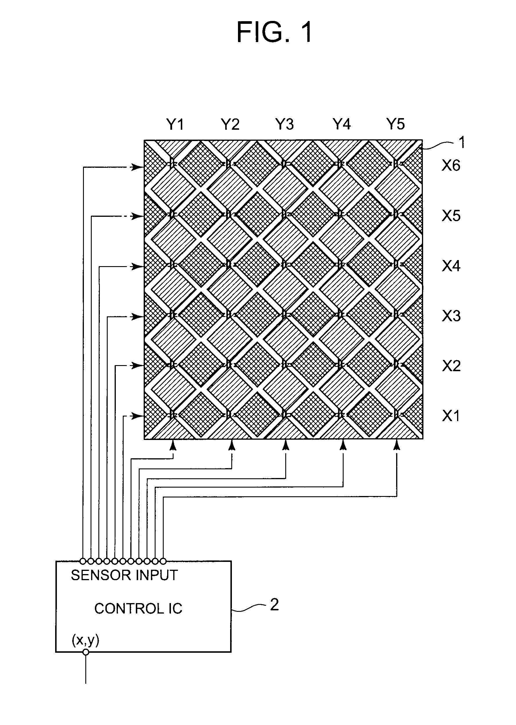
[0055]An exemplary embodiment of the present invention will now be described with reference to the accompanying drawings. FIG. 1 is a diagram illustrating an example of a capacitive touch panel device according to the present invention. As shown in FIG. 1, the capacitive touch panel device includes a capacitive touch panel 1 and a control IC 2, which drives the touch panel 1.
[0056]The touch panel 1 is placed on a transparent substrate made, for instance, of glass or PET film in such a manner that ITO or other transparent electrodes do not overlap with each other. Areas in which sensor lines X1 to X6 extended in the x direction intersect sensor lines Y1 to Y5 extended in the y direction, which is different from the x direction, are provided, for instance, with an insulating layer (not shown) so that there is no conduction between the X1 to X6 sensor lines and Y1 to Y5 sensor lines. It is preferred that the areas of the intersections of the sensor lines be minimized.
[0057]FIG. 1 shows...
PUM
 Abstract
Description
Claims
Application Information