Testing integrated circuits

a technology of integrated circuits and test methods, applied in the direction of measuring devices, instruments, fault locations, etc., can solve the problems of increasing the number of probes needed, the type of test system has several limitations, and the risk of damaging the contact pads of the dies under test, so as to reduce the number of probes

Active Publication Date: 2013-01-22
STMICROELECTRONICS SRL
View PDF7 Cites 16 Cited by
  • Summary
  • Abstract
  • Description
  • Claims
  • Application Information

AI Technical Summary

Benefits of technology

[0020]The Applicant has found that a way to reduce the number of probes necessary to perform the test of an IC is to employ a mixing of multiple test stimuli and / or test response signals over the same physical communication channel between the probe card and an IC under test.

Problems solved by technology

However, this type of test system has several limitations.
For example, there is the risk of damaging the contact pads of the dies under test.
As known, a contact pad includes of an enlarged metallization region of the IC; when the tip of the mechanical probes touches the pads, there is always the risk that one or more of the pads are damaged by scrubbing, and the likelihood that this happens increases with the number of probes.
Also, the parallel-testing capability is relatively low: indeed, when several dies at a time have to be tested, the number of mechanical probes significantly increases; fabricating probe cards with many probes is not an easy task, and the finite dimensions of the probes pose a physical limit to the density of probes per unit area.
Moreover, the higher the number of probes required, the more probable it is that the electrical contacts between the pads of the ICs under test and the mechanical probes are not good, and electrical discontinuities may take place, which affect the test results.
Furthermore, when the contact pads are very close to each other (a situation frequently encountered due to the constant increase in integration scale and size shrinking), it is very difficult to ensure a good physical contact of the mechanical probes with the contact pads.
Such a problem is emphasized when the pads are small in size and / or a large number thereof is present on each die.
In addition, the mechanical probes are very expensive, thus producing probe cards with several probes negatively contributes to the increase of the overall cost of the test system, and eventually of the ICs.
This constraint heavily reduces the communication efficiency, sensibly increasing test time and test costs.

Method used


Image

  • Testing integrated circuits
  • Testing integrated circuits
  • Testing integrated circuits

Examples


Embodiment Construction

[0036]Throughout the following description, identical or similar elements in the drawings are denoted by same reference numerals.

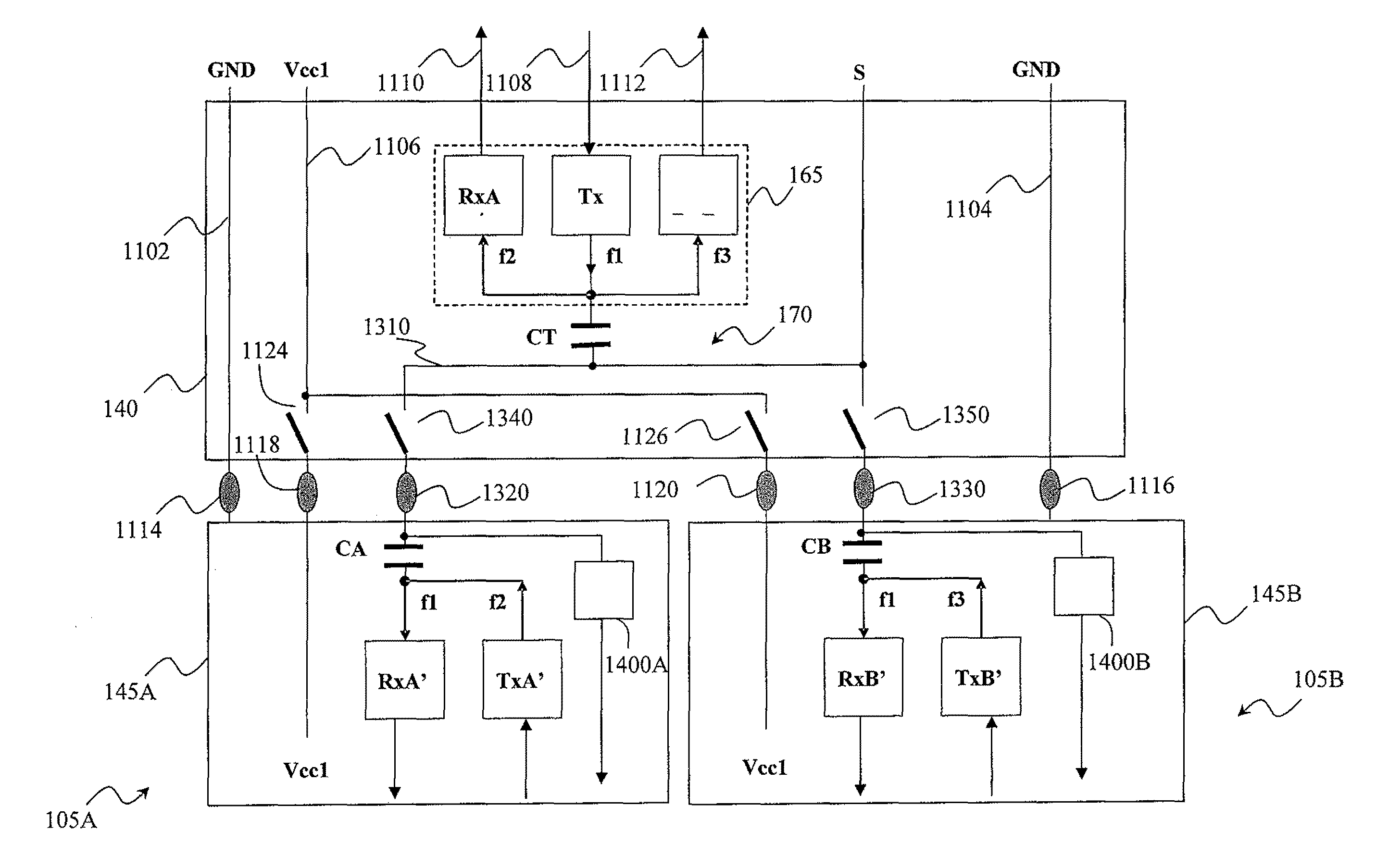
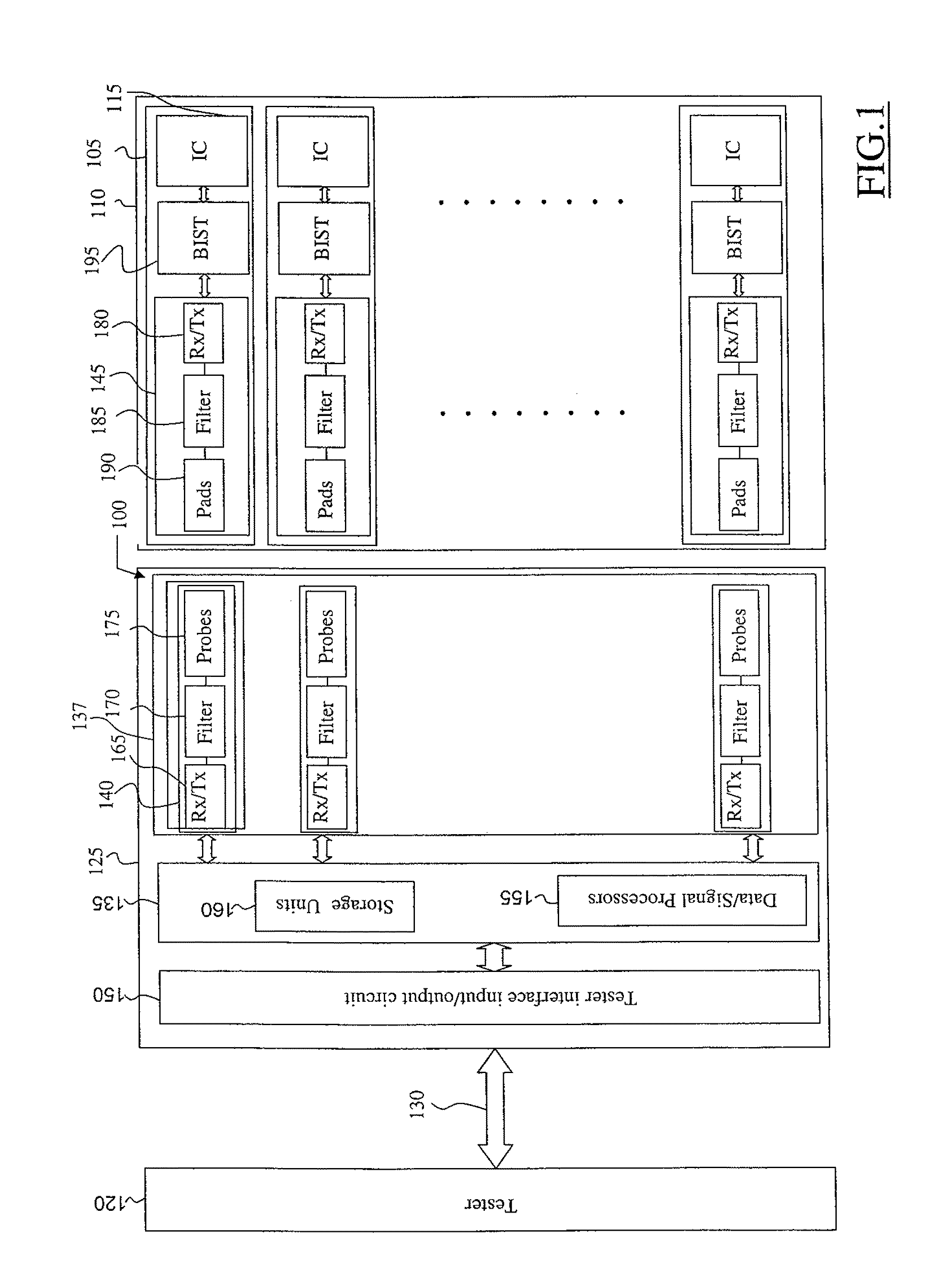
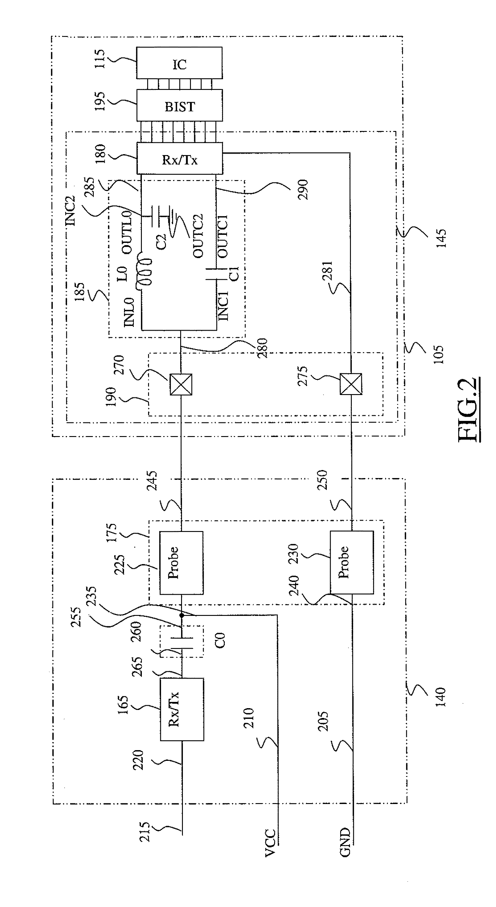
[0037]Referring to FIG. 1, a block diagram of a test system 100 according to an embodiment of the present invention is schematically shown. The test system 100 is adapted to perform the wafer-level testing of a plurality (for example, hundreds) of IC dies 105 belonging to a semiconductor wafer 110, prior to the dicing thereof into individual chips.

[0038]The specific type of IC 115 integrated on the dies 105 is not limitative of the present invention; in particular, and merely by way of example, the ICs 115 may be or include memory devices, microprocessors or microcontrollers, Digital Signal Processors (DSPs), digital logic circuits, Application Specific Integrated Circuits (ASICs), Field Programmable Gate arrays (FPGAs), analog circuits, RF circuits, MEMS (Micro ElectroMechanical Systems).

[0039]For testing the ICs 115 on the dies 105 in order to assess the...


PUM


Abstract

A method of testing integrated circuits is provided. The method includes establishing at least one first physical communication channel between a test equipment and a respective group of integrated circuits under test by having probes of the test equipment contacting at least one corresponding physical contact terminal of each integrated circuit of the respective group. The method further includes having the test equipment exchanging, over the at least one first physical communication channel, the same test stimuli with each integrated circuit of the group. The method still further includes having each integrated circuit of the group establishing a corresponding second physical communication channel with the test equipment by having at least one physical contact terminal of the integrated circuit contacted by a corresponding probe of the test equipment. The method further includes having each integrated circuit of the group exchanging, over the second physical communication channel, a corresponding test response signal based on the received test stimuli with the test equipment. The test stimuli are exchanged by modulating at least one first carrier wave based on the test stimuli; the at least one first carrier wave has at least one first frequency. The test response signals of each integrated circuit of the group are exchanged by modulating at least one respective second carrier wave based on the test response signals; each second carrier wave have at least one respective second frequency.

Description

CROSS REFERENCE TO RELATED APPLICATIONS[0001]This application is a continuation-in-part of U.S. application Ser. No. 12 / 398,148, filed Mar. 4, 2009 entitled “TESTING INTEGRATED CIRCUITS USING FEW TEST PROBES”, which application claims the priority benefit of Italian patent application number MI2008A00365, filed on Mar. 5, 2008, entitled “TESTING INTEGRATED CIRCUITS EXPLOITING FEW TEST PROBES,” which is hereby incorporated by reference to the maximum extent allowable by law.BACKGROUND OF THE INVENTION[0002]1. Field of the Invention[0003]The present invention relates to the field of Integrated Circuits (ICs), and particularly to methods and systems for IC testing.[0004]2. Discussion of the Related Art[0005]ICs are typically manufactured many at a time in the form of dies on a semiconductor material wafer. After manufacturing, the semiconductor wafer is diced, so as to obtain a plurality of individual IC chips.[0006]Before being packaged and shipped to the customers, and installed in v...

Claims


Application Information

Patent Timeline
Patent Type & Authority Patents(United States)
IPC IPC(8): G01R31/02
CPCG01R31/3172G01R31/31905G01R31/31926
Inventor PAGANI, ALBERTO
Owner STMICROELECTRONICS SRL
Why Eureka
Try Eureka