Integrated capacitor with cabled plates

a technology of integrated capacitors and cabled plates, applied in the direction of fixed capacitor details, fixed capacitors, fixed capacitor terminals, etc., can solve the problems of requiring additional steps, requiring large capacitance area, and difficult to integrate in a standard cmos fabrication sequen

Active Publication Date: 2013-01-29
XILINX INC
View PDF122 Cites 25 Cited by
  • Summary
  • Abstract
  • Description
  • Claims
  • Application Information

AI Technical Summary

Benefits of technology

[0008]A capacitor in an integrated circuit (“IC”) has a distribution grid formed in a first patterned metal layer of the integrated circuit and a first vertical conductive filament connected to and extending away from the distribution grid along a first direction. A second vertical conductive filament is connected to the distribution grid and extends in the opposite direction. A first and second grid plates are formed in the metal layers above and below the first patterned metal layer. The grid plates surround the first and second vertical conductive filaments. The distribution grid, first vertical conductive filament and second vertical conductive filament are connected to and form a portion of a first node of the capacitor and the first grid plate and the second grid plate are connected to and form a portion of a second node of the capacitor.

Problems solved by technology

A simple approach is to form two conductive plates with an intervening dielectric; however, this consumes a relatively large area for the capacitance obtained.
Providing an equal number of conductive strips in a layer for each node balances the coupling of each node to the substrate, which is desirable in some applications, but undesirable in others, such as switching applications where it is desirable to have less coupling at one node.
This may be difficult to integrate in a standard CMOS fabrication sequence, and might require additional steps to be added to the standard process flow.

Method used


Image

  • Integrated capacitor with cabled plates
  • Integrated capacitor with cabled plates
  • Integrated capacitor with cabled plates

Examples


Embodiment Construction

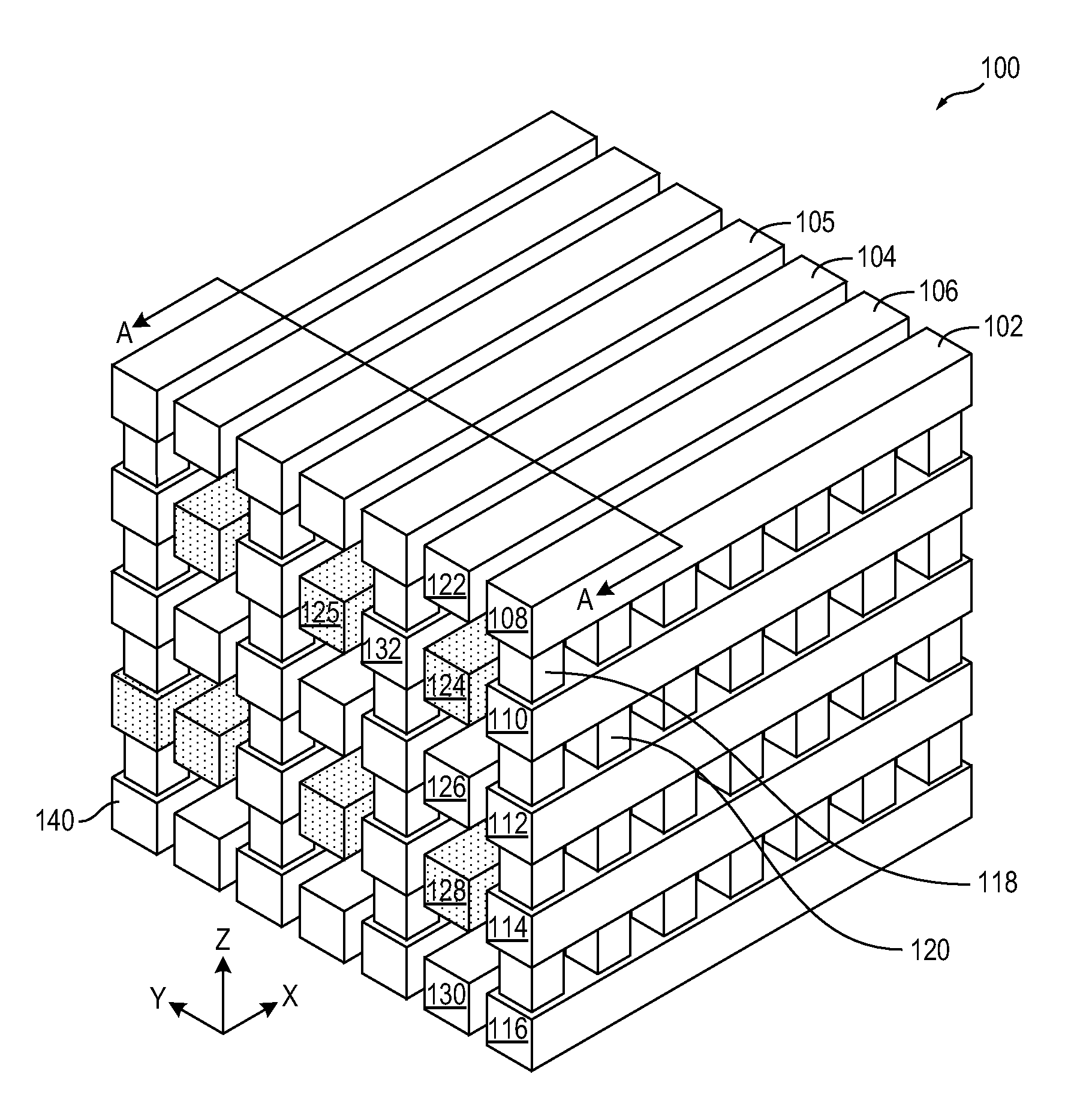
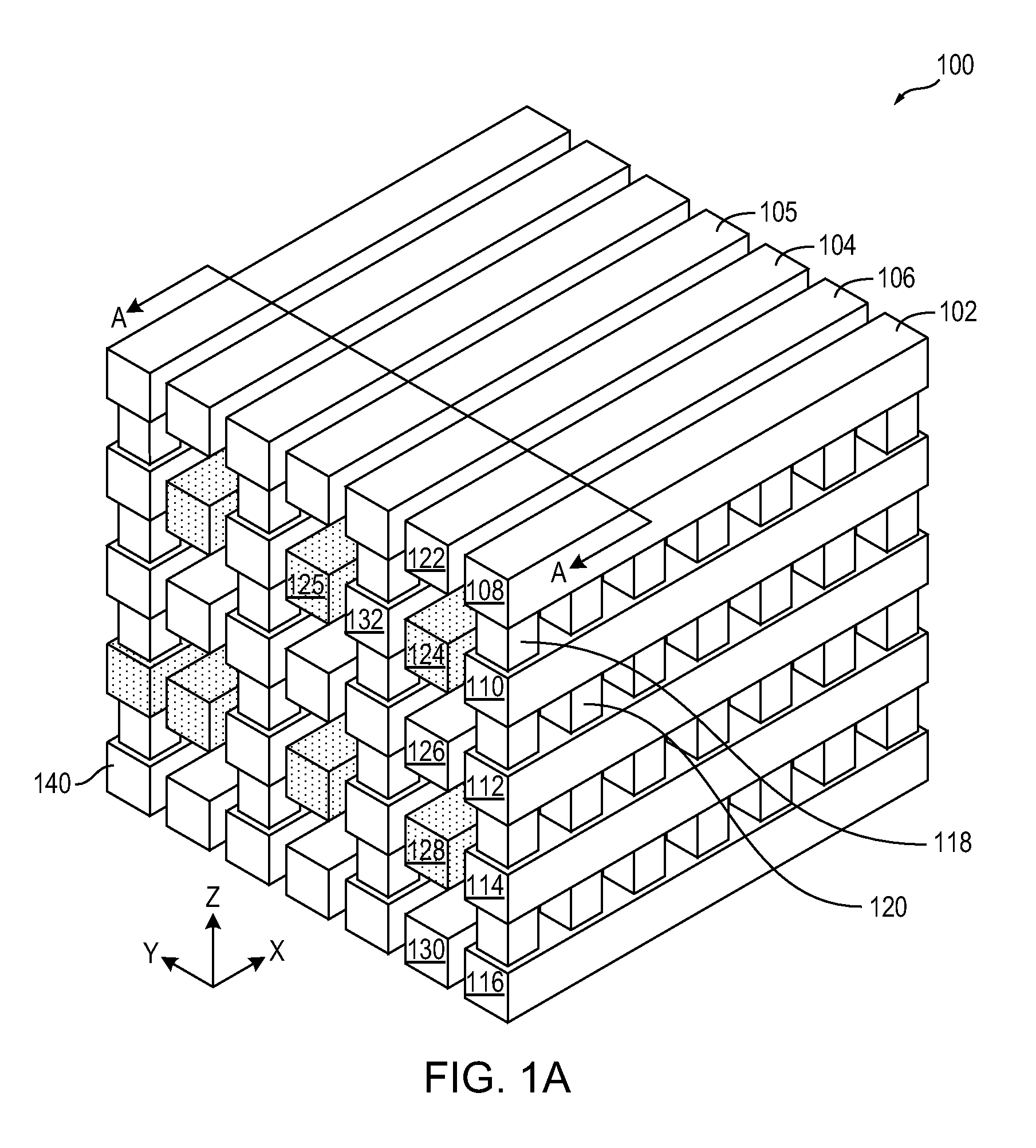
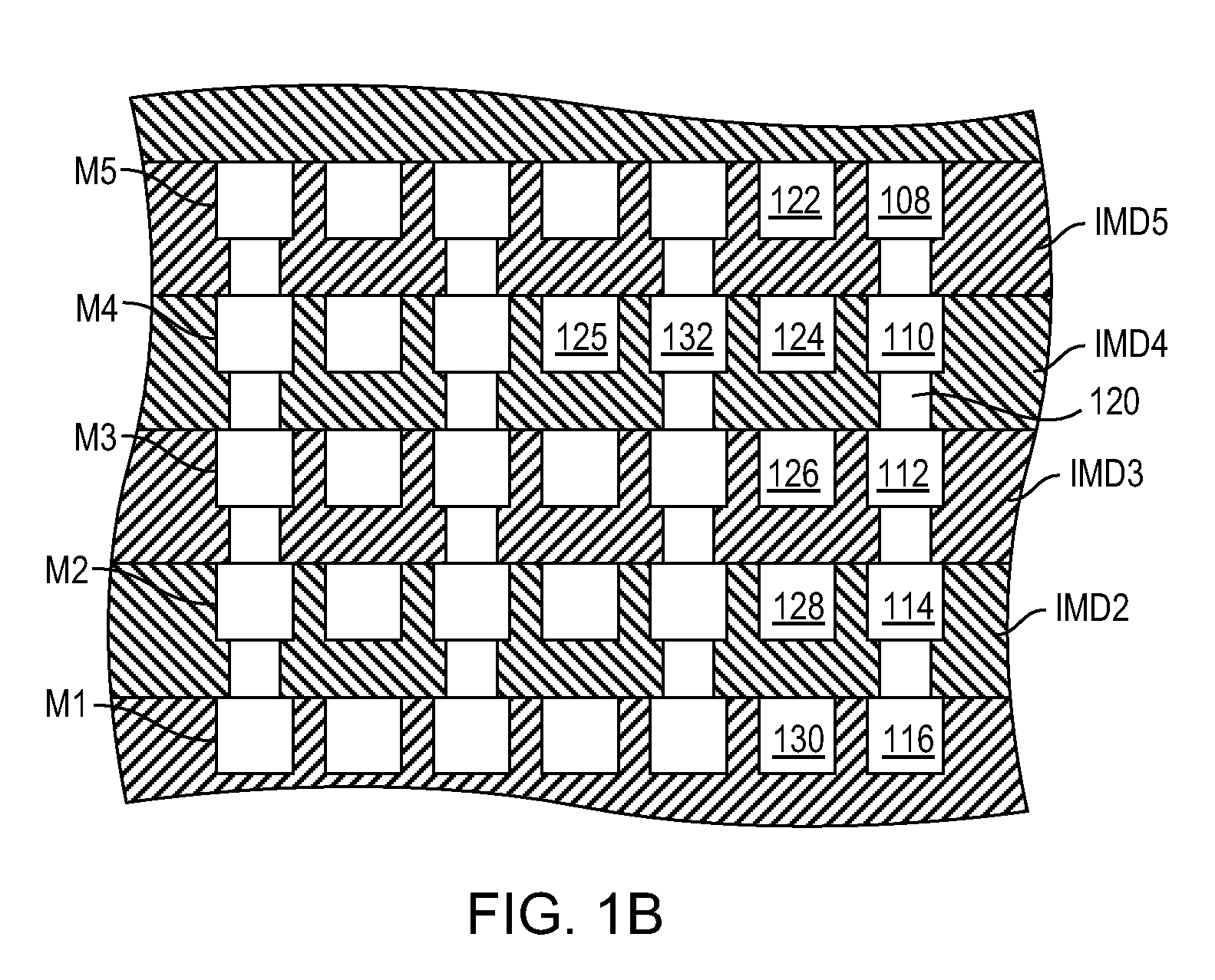
[0018]Complex ICs, such as programmable logic devices, often have several patterned metal layers separated by layers of dielectric material formed over a semiconductor substrate that are used for wiring connections and other functions. Some embodiments of the invention are adaptable to existing CMOS process sequences by using masks that form the desired patterns in the appropriate metal layers and vias through the inter-metal dielectric (“IMD”) layers or inter-layer dielectric (“ILD”). The vias are formed using any of several known techniques, such as contact plug, damascene, or dual damascene techniques. Similarly, the conductive strips are formed using any of several known techniques, such as thin-film metal etch, thin-film metal lift-off, damascene, and dual damascene techniques. In some embodiments, one of the conductive layers is a polysilicon or silicide layer. In a further embodiment, a conductive well in the semiconductor substrate forms a portion of a capacitor plate or a s...


PUM


Abstract

A capacitor in an integrated circuit (“IC”) has a distribution grid formed in a first patterned metal layer of the integrated circuit and a first vertical conductive filament connected to and extending away from the distribution grid along a first direction. A second vertical conductive filament is connected to the distribution grid and extends in the opposite direction. First and second grid plates are formed in the metal layers above and below the first patterned metal layer. The grid plates surround the first and second vertical conductive filaments. The distribution grid, first vertical conductive filament and second vertical conductive filament are connected to and form a portion of a first node of the capacitor and the first grid plate and the second grid plate are connected to and form a portion of a second node of the capacitor.

Description

RELATED APPLICATIONS[0001]This patent application is being concurrently filed with commonly owned U.S. Patent Application entitled SHIELDING FOR INTEGRATED CAPACITORS by Patrick J. Quinn; and with commonly owned U.S. Patent Application entitled INTEGRATED CAPACITOR WITH TARTAN CROSS SECTION by Patrick J. Quinn; and with commonly owned U.S. Patent Application entitled INTEGRATED CAPACITOR WITH INTERLINKED LATERAL FINS by Patrick J. Quinn; and with commonly owned U.S. Patent Application entitled INTEGRATED CAPACITOR WITH ARRAY OF CROSSES by Patrick J. Quinn; and with commonly owned U.S. Patent Application entitled INTEGRATED CAPACITOR WITH ALTERNATING LAYERED SEGMENTS by Jan L. de Jong et al., the disclosures of which are each hereby incorporated by reference in their entireties for all purposes.FIELD OF THE INVENTION[0002]The present invention relates to capacitors formed in integrated circuits (“ICs”) commonly referred to as “integrated capacitors”.BACKGROUND OF THE INVENTION[0003]M...

Claims


Application Information

Patent Timeline
Patent Type & Authority Patents(United States)
IPC IPC(8): H01L21/02
CPCH01G4/228H01G4/232H01L23/5223H01L23/5225H01L27/0207H01L27/0805H01L28/60H01L2924/0002H01L2924/3011H01L2924/00H01L21/02H01L23/52H01L27/02
Inventor QUINN, PATRICK J.
Owner XILINX INC
Why Eureka
Try Eureka