Al technical title is built by PatSnap Al team. It summarizes the technical point description of the patent document.
a technology of integrated mems and cmos, applied in the field of integrated devices, can solve the problems of increasing the cost of mems, focusing on mems development, and reducing costs, and achieve the effect of increasing the yield of devices in dies and being convenient to us
Active Publication Date: 2013-03-12
MOVELLA INC
View PDF26 Cites 43 Cited by
Summary
Abstract
Description
Claims
Application Information
AI Technical Summary
This helps you quickly interpret patents by identifying the three key elements:
Problems solved by technology
Method used
Benefits of technology
[0012]Many benefits are achieved by way of the present invention over conventional techniques. For example, the present technique provides an easy to use process that relies upon conventional technology. In some embodiments, the method provides higher device yields in dies per wafer with the integrated approach. Additionally, the method provides a process and system that are compatible with conventional pro
Problems solved by technology
Although highly successful, ICs and in particular MEMS still have limitations.
Similar to IC development, MEMS development, which focuses on increasing performance, reducing size, and decreasing cost, con
Method used
Image
Click on the blue label to locate the original text in one second.
Reading with bidirectional positioning of images and text.
Examples
Embodiment Construction
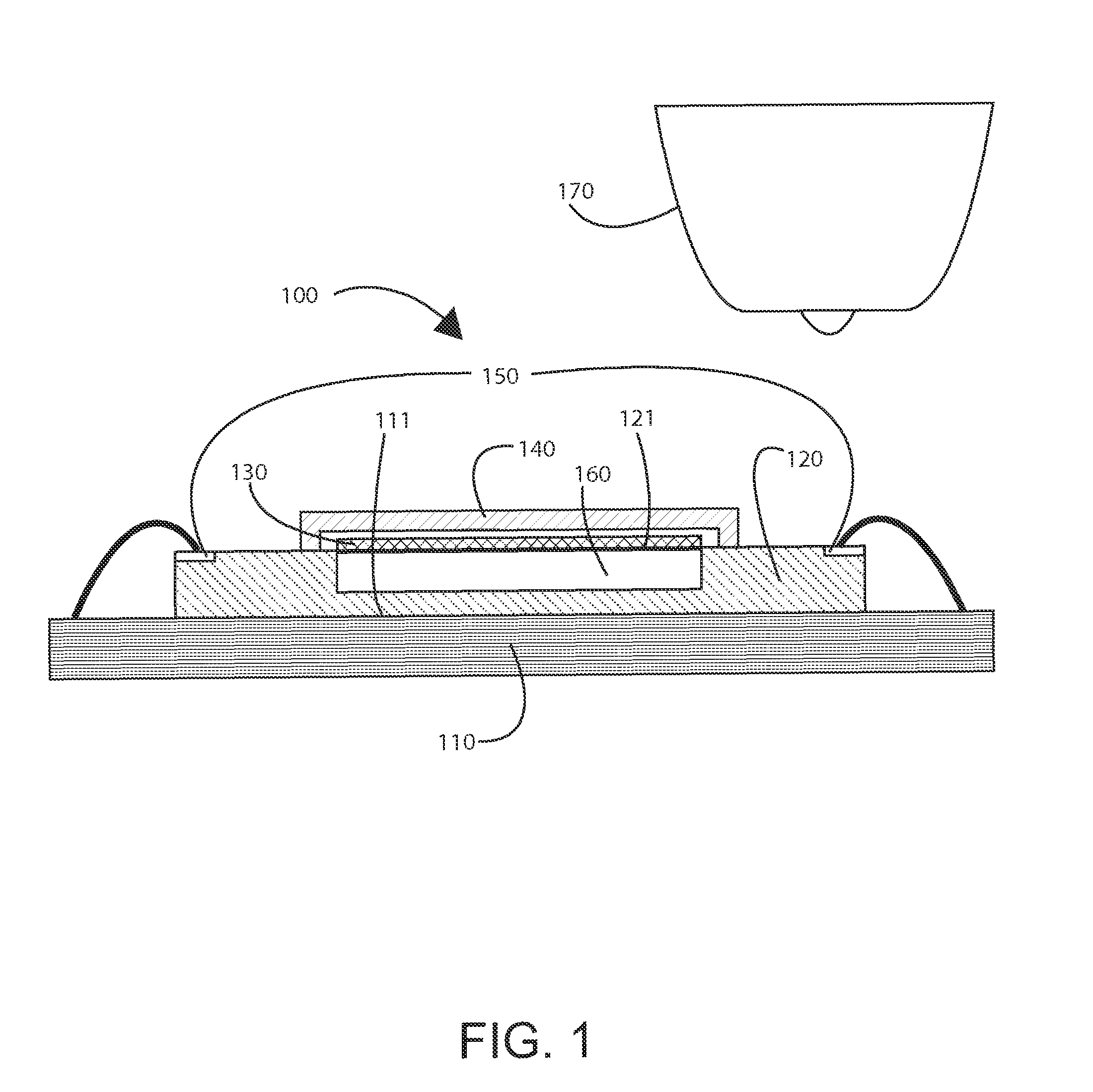
[0027]According to the present invention, techniques related generally to packaging are provided. The present invention relates generally to packaging techniques. More particularly, the present invention provides an improved package for integrated circuits and micro-electrical mechanical systems, commonly termed MEMS. Merely by way of example, the MEMS devices can include at least an accelerometer, a gyroscope, a magnetic sensor, a pressure sensor, a microphone, a humidity sensor, a temperature sensor, a chemical sensor, a biosensor, an inertial sensor, and others. Additionally, the other applications include at least a sensor application or applications, system applications, and broadband applications, among others. But it will be recognized that the invention has a much broader range of applicability.
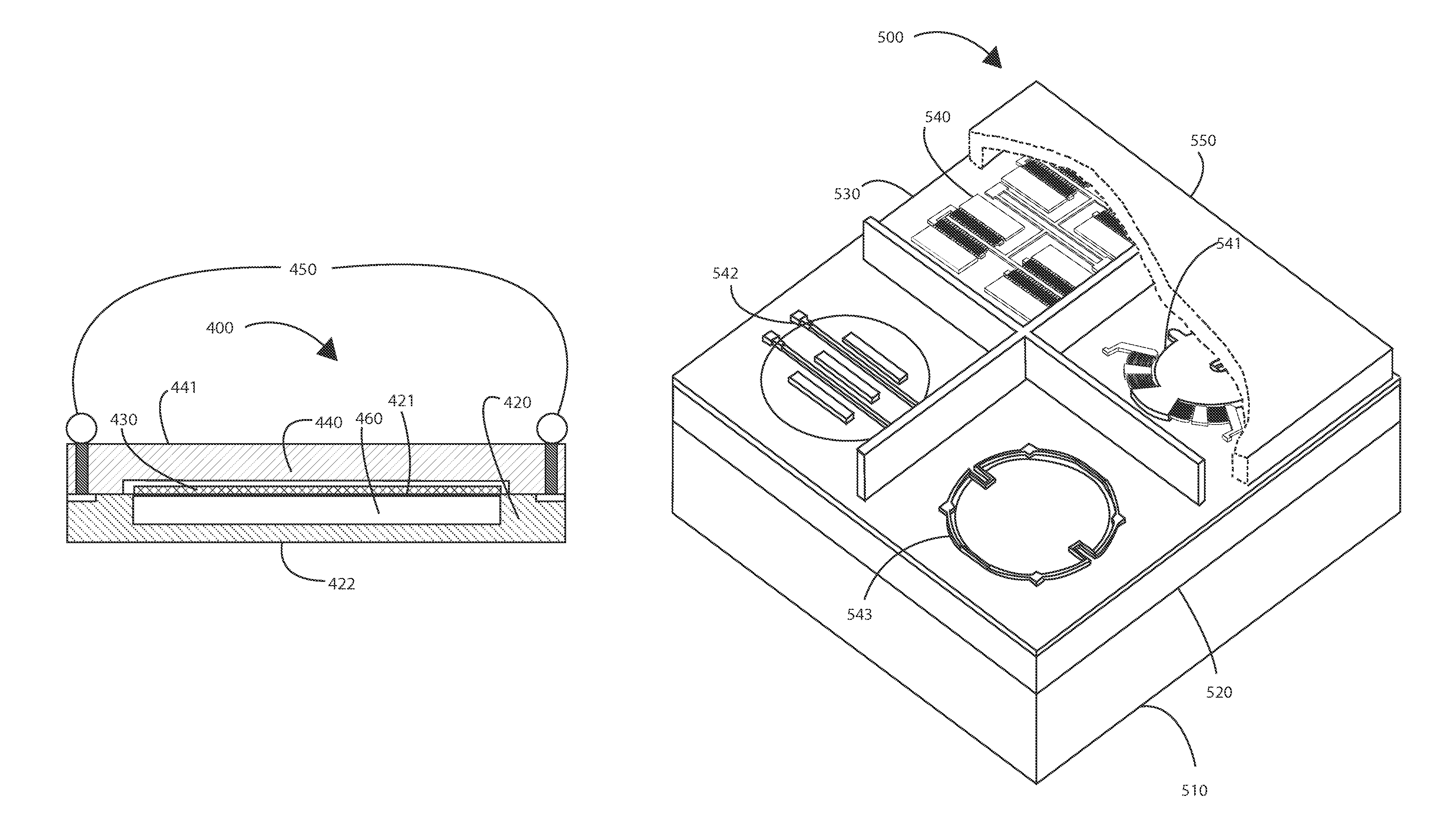
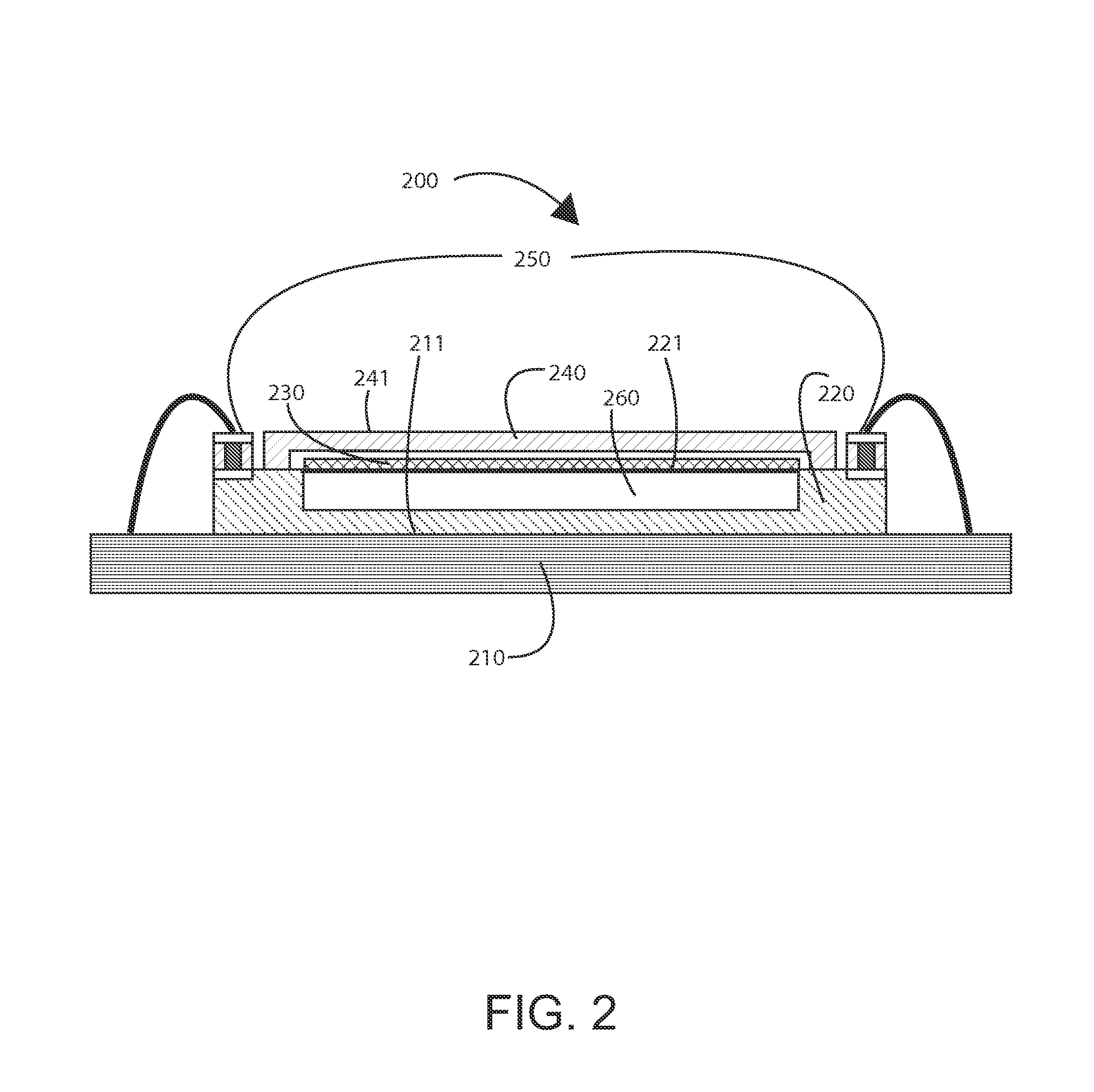
[0028]FIG. 1 is a simplified diagram of an electronic packaging according to a conventional device. As shown, the apparatus 100 includes a substrate member 110, a semiconductor substr...
PUM
Abstract
An apparatus for packaging MEMS and ICs can include a semiconductor substrate, one or more MEMS devices, an enclosure, and one or more bonding structures. The semiconductor substrate can be bonded to a portion of the surface region. The semiconductor substrate can include one or more integrated circuits. Also, the semiconductor substrate can have an upper surface region. The one or more MEMS devise can overlie an inner region of the upper surface region formed by the semiconductor substrate. The enclosure can house the one or more MEMS devices. The enclosure can overlie a first outer region of the upper surface region. Also, the enclosure can have an upper cover region. The one or more bonding structures can be provided within a second outer region of the supper surface region.
Description
CROSS-REFERENCES TO RELATED APPLICATIONS[0001]The present application claims priority to and incorporates by reference, for all purposes, the following pending patent application: U.S. Pat. App. No. 61 / 260,847, filed Nov. 13, 2009. The present invention also incorporates by reference, for all purposes, the following co-pending patent applications related to sensor and MEMS devices: U.S. patent application Ser. No. 12 / 859,631, filed Aug. 19, 2010, U.S. Pat. App. No. 61 / 356,467, filed Jun. 18, 2010, U.S. patent application Ser. No. 12 / 859,672, filed Aug. 19, 2010, U.S. patent application Ser. No. 12 / 859,647, filed Aug. 19, 2010, and U.S. patent application Ser. No. 12 / 913,440, filed Oct. 27, 2010.BACKGROUND OF THE INVENTION[0002]The present invention relates generally to integrated devices. More particularly, the present invention provides a system and method for integrating at least two different micro electro mechanical systems (MEMS) devices with one or more complementary metal oxi...
Claims
Application Information
Patent Timeline
Application Date:The date an application was filed.
Publication Date:The date a patent or application was officially published.
First Publication Date:The earliest publication date of a patent with the same application number.
Issue Date:Publication date of the patent grant document.
PCT Entry Date:The Entry date of PCT National Phase.
Estimated Expiry Date:The statutory expiry date of a patent right according to the Patent Law, and it is the longest term of protection that the patent right can achieve without the termination of the patent right due to other reasons(Term extension factor has been taken into account ).
Invalid Date:Actual expiry date is based on effective date or publication date of legal transaction data of invalid patent.