Plasma display device and method of driving plasma display panel

a display device and plasma technology, applied in the field of plasma display devices and driving plasma display panels, can solve the problems of insufficient reduction of the maximum voltage of all-cell initialization operation, disadvantageous emission of light, etc., and achieve the effect of reducing black luminance and sharpening contras

Inactive Publication Date: 2013-03-19
PANASONIC CORP
View PDF10 Cites 0 Cited by
  • Summary
  • Abstract
  • Description
  • Claims
  • Application Information

AI Technical Summary

Benefits of technology

[0026]Thus, in displaying the predetermined image, occurrence of the initializing bright point can be suppressed to reduce the maximum voltage in an all-cell initializing operation, light emission in the all-cell initializing operation is suppressed to reduce the black luminance, and the contrast can be sharpened.

Problems solved by technology

When the maximum voltage in the all-cell initializing operation is reduced, however, priming generated during initialization decreases to cause strong discharge in the initializing operation in the next field, sustaining discharge occurs though writing has not been performed, and a discharge cell (hereinafter referred to as “initializing bright point”) that emits light can be generated disadvantageously.
Therefore, the maximum voltage in all-cell initializing operation cannot be sufficiently reduced.

Method used


Image

  • Plasma display device and method of driving plasma display panel
  • Plasma display device and method of driving plasma display panel
  • Plasma display device and method of driving plasma display panel

Examples


Embodiment Construction

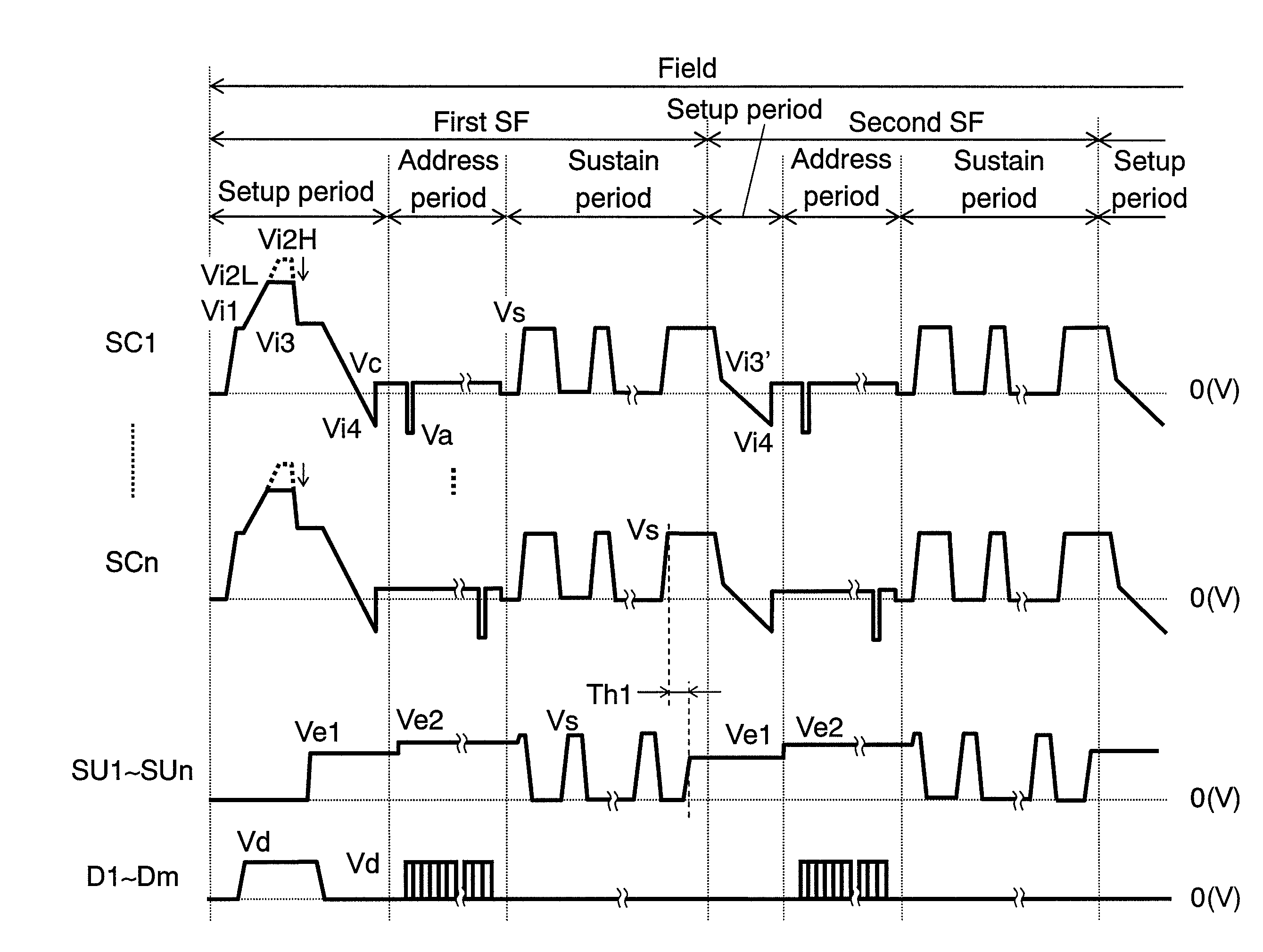
[0066]A plasma display device in accordance with an exemplary embodiment of the present invention will be described hereinafter with reference to the accompanying drawings.

Exemplary Embodiment

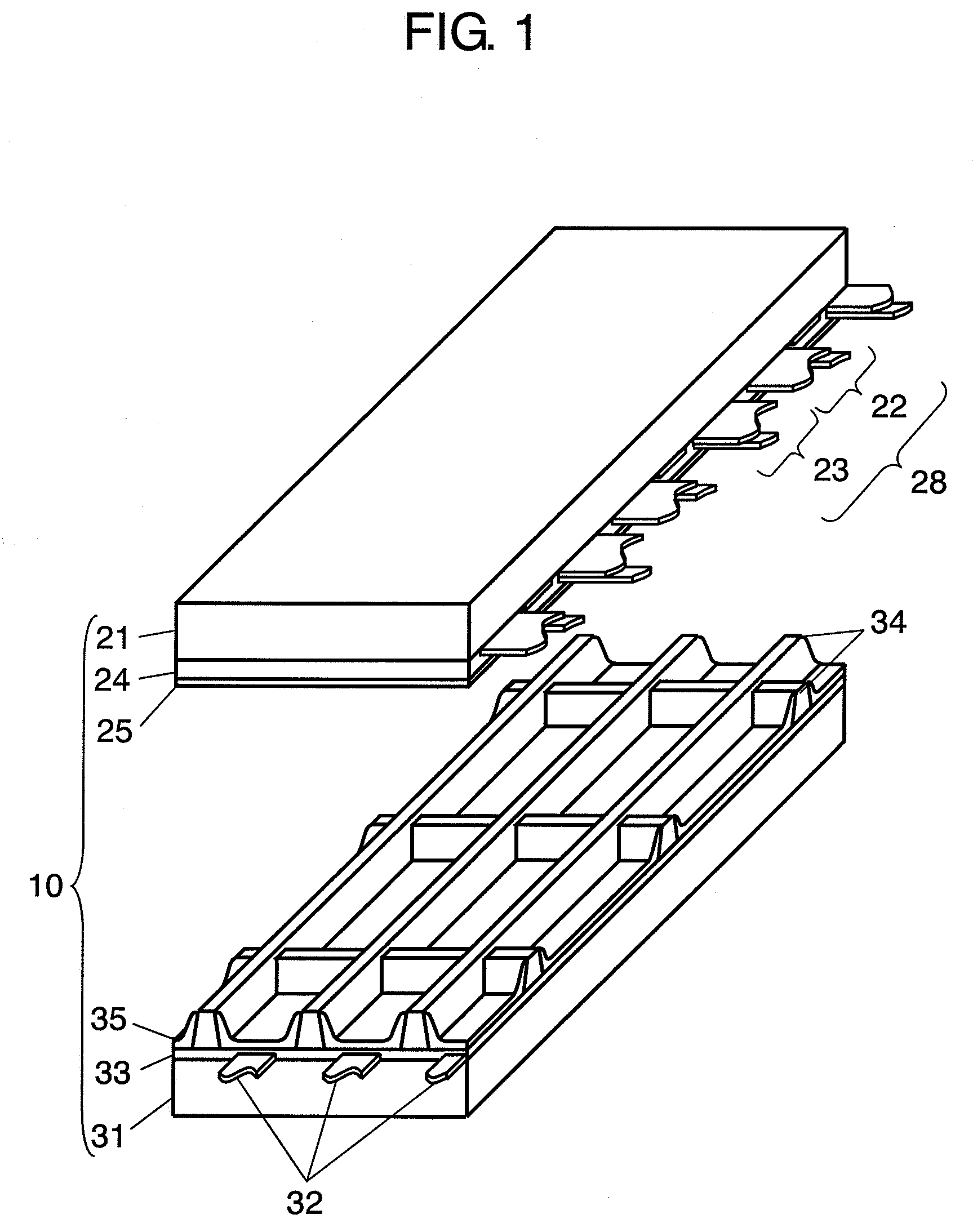
[0067]FIG. 1 is an exploded perspective view showing a structure of panel 10 in accordance with the exemplary embodiment of the present invention. A plurality of display electrode pairs 28 formed of scan electrodes 22 and sustain electrodes 23 are disposed on glass-made front plate 21. Dielectric layer 24 is formed so as to cover scan electrodes 22 and sustain electrodes 23, and protective layer 25 is formed on dielectric layer 24.

[0068]Protective layer 25 is actually used as a material of the panel in order to reduce the discharge start voltage in a discharge cell. Protective layer 25 is made of material that is mainly made of MgO and has a large secondary electron discharge coefficient and high durability when neon (Ne) and xenon (Xe) gases are filled.

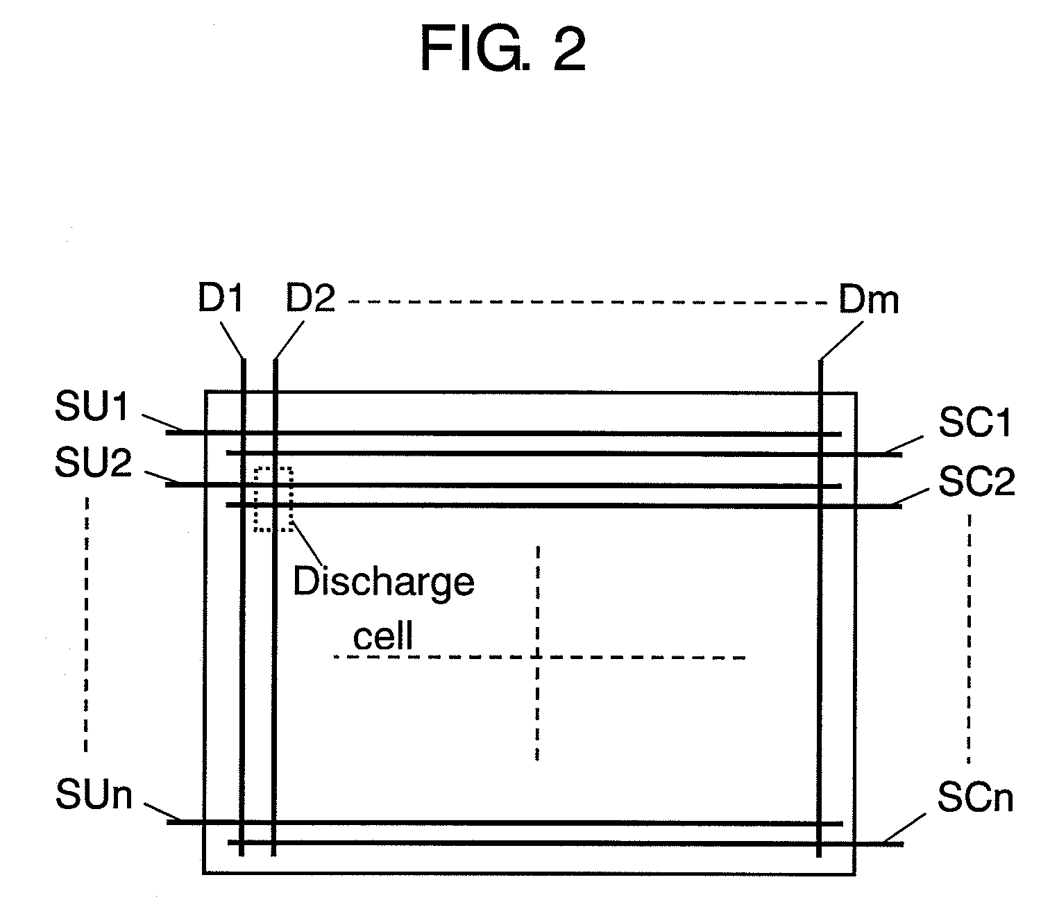
[0069]A plurality of data electrodes 32 a...


PUM


Abstract

In displaying a predetermined image on a plasma display panel, occurrence of an initializing bright point can be suppressed to reduce the maximum voltage in an all-cell initializing operation, light emission in the all-cell initializing operation is suppressed to reduce the black luminance, and the contrast is sharpened. In driving the plasma display panel, one field period includes a plurality of subfields having a setup period for causing initializing discharge in discharge cells, an address period, and a sustain period. One field period includes at least one subfield for applying ramp waveform voltage increasing in the setup period to the scan electrodes. The maximum voltage of the ramp waveform voltage can be varied. When a predetermined image establishing a previously determined condition is displayed, the ramp waveform voltage is generated whose maximum voltage is smaller than when an image other than the predetermined image is displayed, and a positive voltage is applied to the data electrodes at least while the ramp waveform voltage having the smaller maximum voltage is applied to the scan electrodes.

Description

TECHNICAL FIELD[0001]The present invention relates to a plasma display device used in a wall-hanging television (TV) or a large monitor, and a driving method of a plasma display panel.BACKGROUND ART[0002]A typical alternating-current surface discharge type panel used as a plasma display panel (hereinafter referred to as “panel”) has many discharge cells between a front plate and a back plate that are faced to each other. The front plate has the following elements:[0003]a plurality of display electrode pairs disposed in parallel on a front glass substrate; and[0004]a dielectric layer and a protective layer for covering the display electrode pairs.Here, each display electrode pair is formed of a pair of scan electrode and sustain electrode. The back plate has the following elements:[0005]a plurality of data electrodes disposed in parallel on a back glass substrate;[0006]a dielectric layer for covering the data electrodes;[0007]a plurality of barrier ribs disposed on the dielectric lay...

Claims


Application Information

Patent Timeline
Patent Type & Authority Patents(United States)
IPC IPC(8): G09G3/28G09G3/292G09G3/20G09G3/291G09G3/293G09G3/298
CPCG09G3/2927G09G3/296H04N5/70G09G3/2022G09G2310/066G09G2320/0238G09G2320/041G09G2330/028G09G2360/16H01J11/12
Inventor SHOJI, HIDEHIKOORIGUCHI, TAKAHIKO
Owner PANASONIC CORP
Why Eureka
Try Eureka