High Voltage Tolerant Output Buffer

An output buffer, high-voltage technology, applied in the direction of logic circuit connection/interface layout, logic circuit coupling/interface using field effect transistors, etc., to avoid instability and ensure normal operation.

Active Publication Date: 2011-11-30
SEMICON MFG INT (SHANGHAI) CORP
View PDF0 Cites 0 Cited by
  • Summary
  • Abstract
  • Description
  • Claims
  • Application Information

AI Technical Summary

Problems solved by technology

[0004] The technical problem to be solved by the present invention is to provide an output buffer that can withstand high voltage, so as to solve the problem that the standard output buffer in this type of circuit in the prior art is used for open-drain purposes and has an intermediate level in the process of switching to a high level. The problem

Method used


Image

  • High Voltage Tolerant Output Buffer
  • High Voltage Tolerant Output Buffer
  • High Voltage Tolerant Output Buffer

Examples


Embodiment Construction

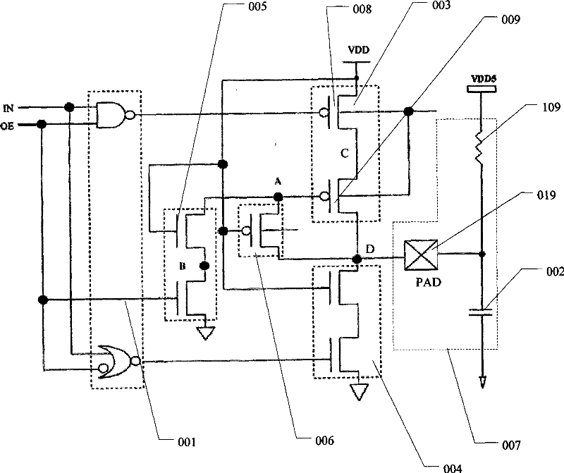
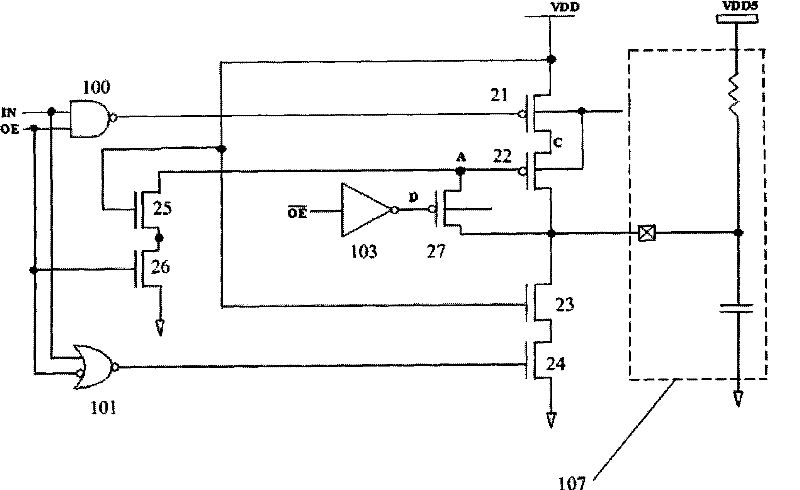
[0027] Please refer to figure 2 , figure 2It is the circuit diagram of the output buffer of the present invention that can withstand high voltage, it includes an input module, the input terminal is connected to the input signal (IN) and the output enable signal (OE), and includes a NAND gate 100 and a NOR gate 101, so The input terminals of the NAND gate 100 are IN and OE, and the input terminals of the NOR gate 101 are IN and OE; the pull-up module receives the first output signal of the input module, between the first voltage and the output point A high-impedance or low-impedance circuit is provided according to the received signal, the pull-up module includes a first transistor 21 and a second transistor 22, the gate of the first transistor 21 is connected to the output terminal of the NAND gate 100, The drain of the first transistor 21 is connected to the source of the second transistor 22, the first transistor 21 and the second transistor 22 are used for pull-up, and t...


PUM


Abstract

The invention provides an output buffer capable of withstanding high voltage, which includes an input module, a pull-up module, a pull-down module, an enabling control module and a voltage limiting module, the input terminal of the input module is connected with an input signal and an output enabling signal, and The voltage module is connected with an inverter, the output signal of the inverter controls the conduction of the voltage limiting module, and the input signal of the inverter is the negation of the output enable signal. The present invention effectively improves the standard input and output circuit as an open leakage circuit. The performance of the output waveform during the circuit, while reducing the maximum voltage on the voltage limiting transistor, improving the reliability of the circuit, thus ensuring the stable operation of the entire circuit.

Description

technical field [0001] The invention relates to the field of semiconductor integrated circuits, in particular to an output buffer capable of withstanding high voltage. Background technique [0002] Buffer registers are also called buffers, which are divided into input buffers and output buffers. The function of the former is to temporarily store the data sent by the peripheral so that the processor can take it away; the function of the latter is to temporarily store the data sent by the processor to the peripheral. With the numerical control buffer, the high-speed working CPU and the slow-working peripherals can coordinate and buffer, and realize the synchronization of data transmission. Since the buffer is connected to the data bus, it must have a three-state output function. In addition, the output buffer can also amplify the signal to play the role of driving, and also has the function of isolation. For example, taking the mos circuit as an example, each integrated circ...

Claims


Application Information

Patent Timeline
Patent Type & Authority Patents(China)
IPC IPC(8): H03K19/0175H03K19/0185
Inventor 俞大立郭之光程惠娟陈先敏陈捷
Owner SEMICON MFG INT (SHANGHAI) CORP
Why Eureka
Try Eureka