On chip dynamic read for non-volatile storage

a dynamic read and non-volatile storage technology, applied in static storage, digital storage, instruments, etc., can solve the problems of large computation requirements, read errors can occur, and voltage distribution of a s

Active Publication Date: 2013-03-26
SANDISK TECH LLC
View PDF8 Cites 35 Cited by
  • Summary
  • Abstract
  • Description
  • Claims
  • Application Information

AI Technical Summary

Problems solved by technology

However, the read reference voltages are typically fixed and do not account for the fact that the threshold voltage distribution of a set of storage elements can change, e.g., due to factors such as charge leakage, temperature changes, number of programming cycles and the like.
As a result, read errors can occur.
However, this requires substantial computations, which may be time consuming.
Both transferring the data out of the memory array

Method used


Image

  • On chip dynamic read for non-volatile storage
  • On chip dynamic read for non-volatile storage
  • On chip dynamic read for non-volatile storage

Examples


Embodiment Construction

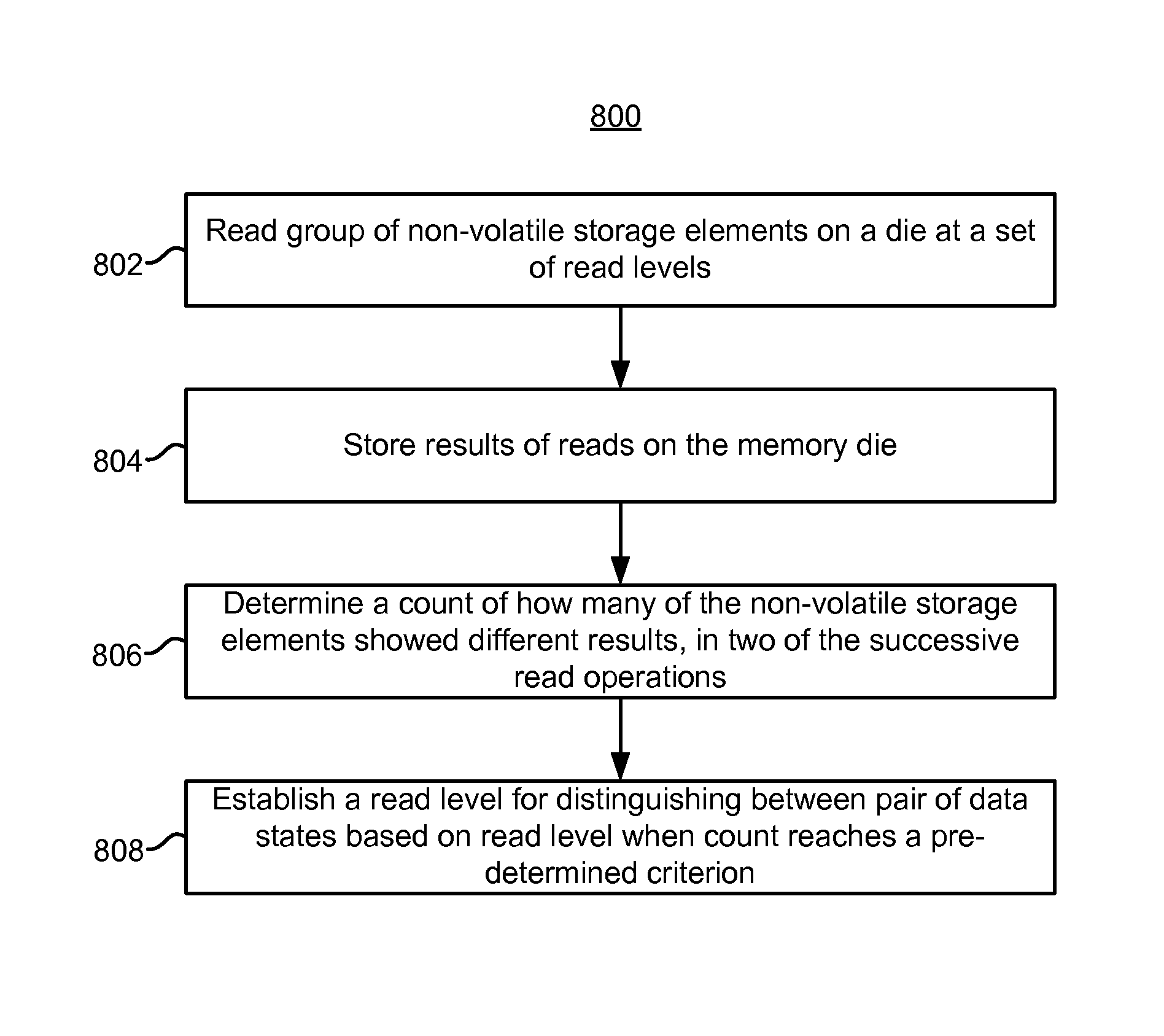
[0034]Dynamically determining read levels on chip (e.g., memory die) is disclosed herein. In one embodiment, an initial read of non-volatile storage elements (e.g., memory cells) is performed at a default read level. Note that this read may determine whether each memory cell has a threshold voltage above or below the read level. Results of the read may be stored in a first set of data latches on the memory die. Then, the read level may be adjusted slightly prior to reading again. Results of the second read may be stored in a second set of data latches. Then, the results in the two sets of data latches may be compared, on a memory cell by memory cell basis. In effect, the comparison may determine which memory cells showed a different result for the two reads (e.g., “mis-compares”). If the number of mis-compares is not less than a pre-determined threshold, then another read may be performed at another read level. When the number of mis-compares is less than the pre-determined threshol...


PUM


Abstract

Dynamically determining read levels on chip (e.g., memory die) is disclosed herein. One method comprises reading a group of non-volatile storage elements on a memory die at a first set of read levels. Results of the two most recent of the read levels are stored on the memory die. A count of how many of the non-volatile storage elements in the group showed a different result between the reads for the two most recent read levels is determined. The determining is performed on the memory die using the results stored on the memory die. A dynamic read level is determined for distinguishing between a first pair of adjacent data states of the plurality of data states based on the read level when the count reaches a pre-determined criterion. Note that the read level may be dynamically determined on the memory die.

Description

BACKGROUND[0001]The present disclosure relates to technology for non-volatile memory.[0002]Semiconductor memory has become more popular for use in various electronic devices. For example, non-volatile semiconductor memory is used in personal navigation devices, cellular telephones, digital cameras, personal digital assistants, mobile computing devices, non-mobile computing devices and other devices. Electrical Erasable Programmable Read Only Memory (EEPROM) and flash memory are among the most popular non-volatile semiconductor memories.[0003]Both EEPROM and flash memory utilize a floating gate that is positioned above and insulated from a channel region in a semiconductor substrate. The floating gate and channel regions are positioned between the source and drain regions. A control gate is provided over and insulated from the floating gate. The threshold voltage of the transistor is controlled by the amount of charge that is retained on the floating gate. That is, the minimum amount...

Claims


Application Information

Patent Timeline
IPC IPC(8): G11C11/34G11C16/04G11C16/06
CPCG11C11/5642G11C16/26G11C16/04G11C16/3495G11C2211/5644G11C16/3418
Inventor DUTTA, DEEPANSHULEE, DANALUTZE, JEFFREY
Owner SANDISK TECH LLC
Why Eureka
Try Eureka