Electronic device having thermally managed electron path and method of thermal management of very cold electrons

a technology of electron path and electron thermal management, which is applied in the field of thermal management, can solve the problems of electron decoupling significantly, inability to remove heat thereafter generated, and complex thermal management at such very low temperatures, and achieve the effect of increasing the potential energy density of conduction charge carrier

Active Publication Date: 2013-04-16
WSOU INVESTMENTS LLC
View PDF4 Cites 1 Cited by
  • Summary
  • Abstract
  • Description
  • Claims
  • Application Information

AI Technical Summary

Benefits of technology

[0007]Another aspect of the invention provides a method of operating an electronic device. In one embodiment, the method includes moving a charge to a conductive region to substantially increase a potential energy of conduction charge carriers in a controllable semiconductor channel of a transistor, the channel being located near the conductive region, the moving causing a density of the conduction charge carriers to be substantially lowered in the channel with respect to the density of said carriers therein in the absence of said charge being moved to the conductive region.

Problems solved by technology

Unfortunately, thermal management at such very low temperatures has proven quite complex and difficult.
Unfortunately, this technique is problematic in that once the electrons enter the device, heat thereafter generated cannot be removed from them.
Unfortunately, electrons begin to decouple significantly from phonons at around 50 mK, at which point lattice cooling begins to be ineffective.
Lattice cooling utterly fails below 10 mK.

Method used


Image

  • Electronic device having thermally managed electron path and method of thermal management of very cold electrons
  • Electronic device having thermally managed electron path and method of thermal management of very cold electrons
  • Electronic device having thermally managed electron path and method of thermal management of very cold electrons

Examples


Embodiment Construction

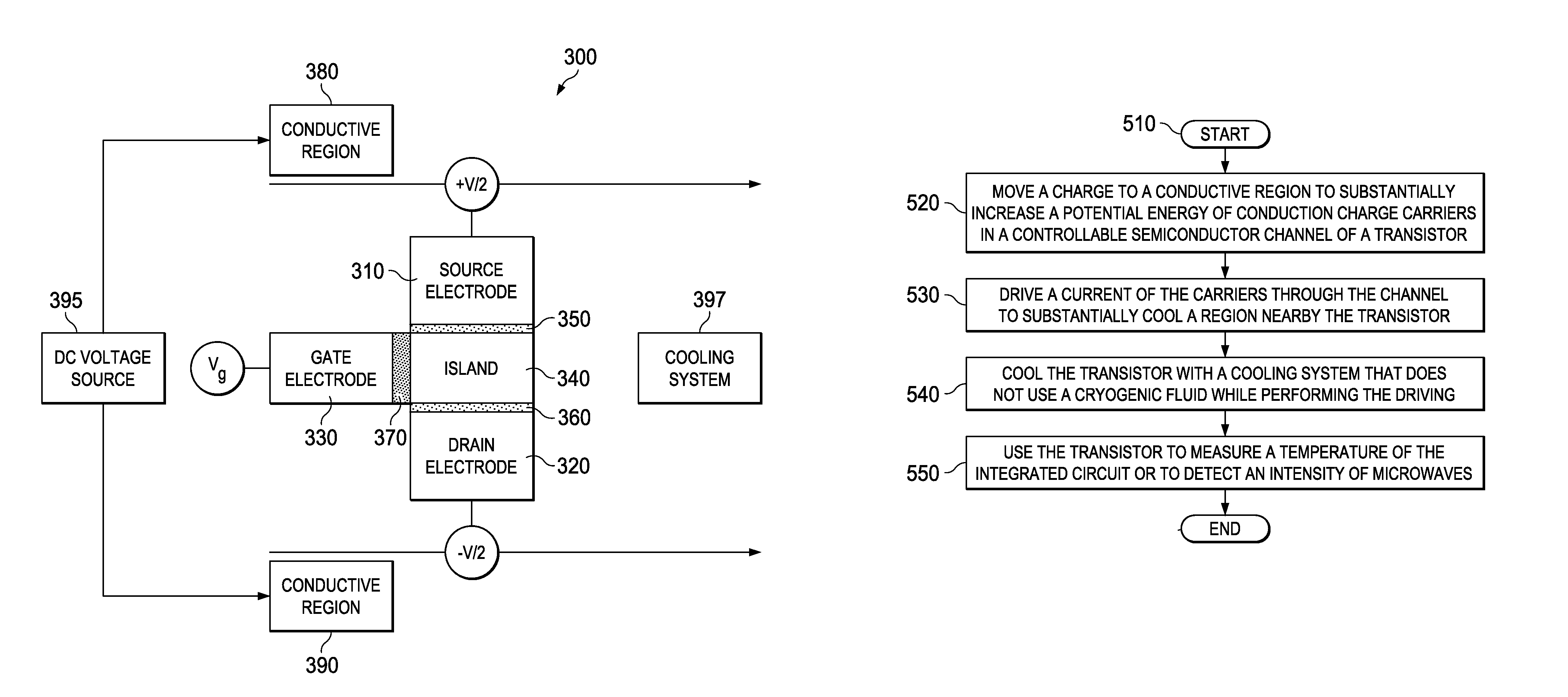
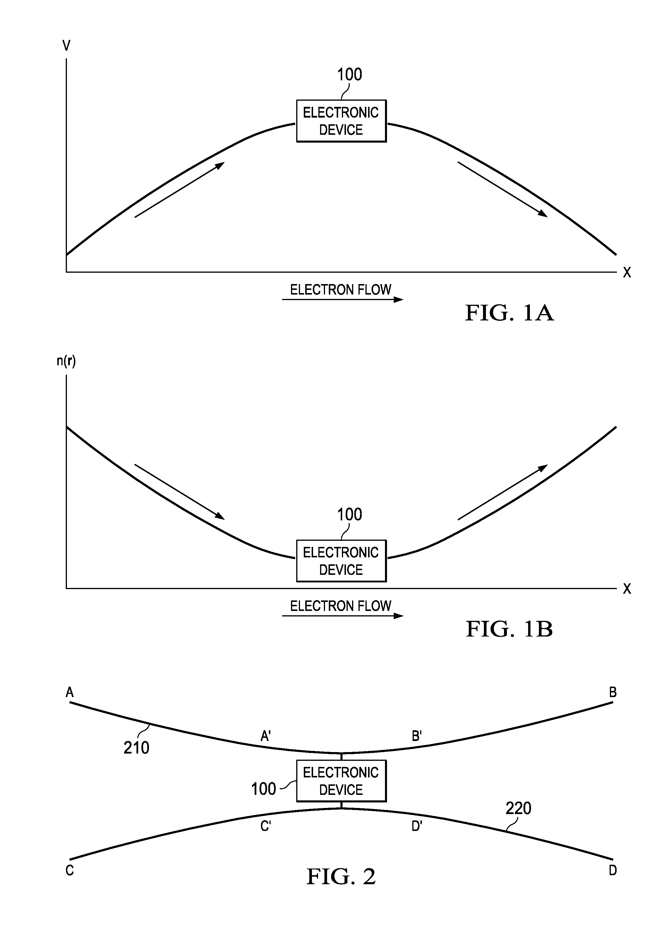
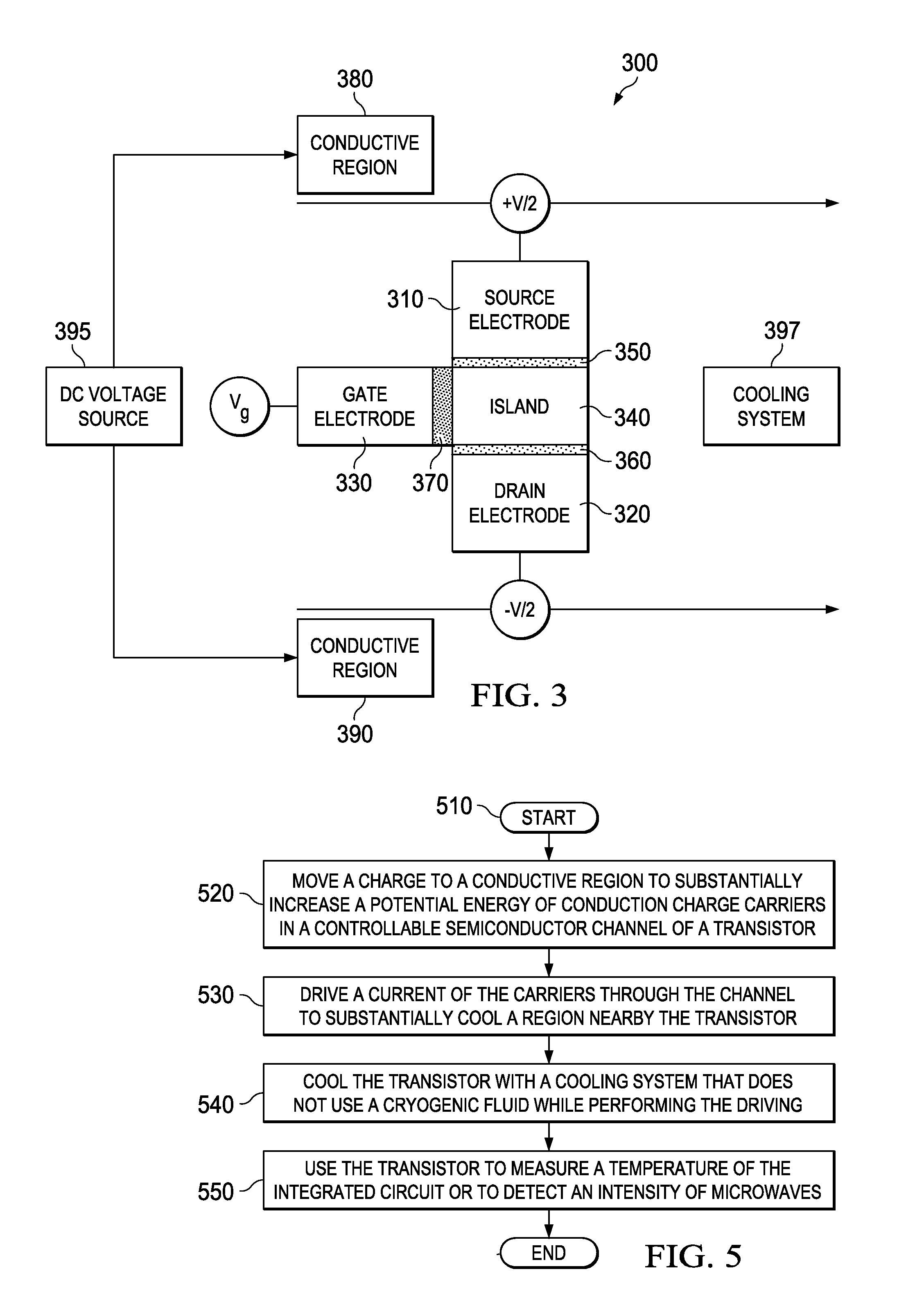
[0014]Disclosed herein are various embodiments of a novel technique for cooling an electronic device. Underlying the embodiments is the novel realization that an electronic device can be cooled by cooling the electrons provided to it by means of thermodynamic expansion. As a general rule, the temperatures of particles can usually be lowered by increasing the separation between the particles, in other words, decompressing them. An ideal particle follows the adiabatic law: (electrochemical potential−electrostatic potential) / T=constant. Thus by increasing the electrostatic potential, the density reduces, and the temperature drops. This holds true for electrons as well.

[0015]One way to decompress electrons is to cause them to flow up a potential hill. The electrons at the top of the potential hill are less dense; as the electrons go up the potential hill, they become cooler. While they will heat up again as they return down the potential hill, certain embodiments separate that return fr...


PUM

PropertyMeasurementUnit
voltageaaaaaaaaaa
electrical potential energyaaaaaaaaaa
electric fieldaaaaaaaaaa

Abstract

A device and a method of thermal management. In one embodiment, the device includes an integrated circuit, including: (1) a conductive region configured to be connected to a voltage source, (2) a transistor having a semiconductor channel with a controllable conductivity and (3) first and second conducting leads connecting to respective first and second ends of said channel, wherein a charge in the conductive region is configured to substantially raise an electrical potential energy of conduction charge carriers in the semiconductor channel and portions of said leads are located where an electric field produced by said charge is substantially weaker than near the semiconductor channel.

Description

TECHNICAL FIELD OF THE INVENTION[0001]The invention is directed, in general, to thermal management and, more specifically, to an electronic device having a thermally managed electron path and method of thermal management of very cold electrons.BACKGROUND OF THE INVENTION[0002]Removing the heat electronic devices generate during operation has always been a concern. Addressing thermal management requires an understanding of the physics of heat generation and transfer (i.e., conduction, convection and radiation). Thermal management of devices operating well above absolute zero (e.g., 150° K. and above) has long been understood. As a result, effective active and passive cooling techniques exist for such devices.[0003]However, many near-future applications for devices, such as quantum computers, will require devices that operate very close to (e.g., within a few degrees Kelvin and perhaps small fractions of a degree of) absolute zero. Unfortunately, thermal management at such very low te...

Claims


Application Information

Patent Timeline
Patent Type & Authority Patents(United States)
IPC IPC(8): H01L23/58H01L21/66
CPCG06F1/20H01L39/02H03H11/00H01L2924/0002H01L2924/00H01L29/7613H10N60/80
Inventor SIMON, STEVEN H.
Owner WSOU INVESTMENTS LLC
Why Eureka
Try Eureka