Power semiconductor module

a technology of semiconductor modules and semiconductor components, applied in the direction of electrical apparatus, printed circuit non-printed electric components association, electrical apparatus contruction details, etc., can solve the problems of enlargement of the circuit board, imposing a relatively high space requirement on the assembly, and complicated circuit board perforation provision, etc., to achieve simple and cost-effective production

Inactive Publication Date: 2013-04-23
SEMIKRON ELECTRONICS GMBH & CO KG
View PDF15 Cites 10 Cited by
  • Summary
  • Abstract
  • Description
  • Claims
  • Application Information

AI Technical Summary

Benefits of technology

[0006]It is an object of the invention to overcome the disadvantages according to the prior art. The intention, in particular, is to provide a power semiconductor module which is compact and can be produced simply and cost-effectively.
[0007]According to the invention, the pressure contact between the contact elements and the contact areas is exerted by at least one electrical component arranged between the springs and one of the load connection elements. In a departure from the prior art, according to the invention it is proposed that the pressure contact is produced by an electrical component supported on the load connection element. For this purpose, the spring exerts a pressure on the component, which pressure is transmitted from there to the load connection element. Since the spring is now arranged above the component, a more compact overall design can be achieved.
[0014]The second load connection element has at least one perforation through which one of the first contact elements and / or a first connection are / is led. The structural size of the power semiconductor module can thus be reduced further.
[0015]The connections may be soldered or welded to the contact elements. However, it may also be the case that the connections are clamped between the contact areas and the contact elements. That simplifies the production of the power semiconductor module. A clamping force for holding the connections is expediently produced by the spring, which forces the contact elements against the contact areas.

Problems solved by technology

The relative positioning of the spring element and the components imposes a relatively high space requirement on the assembly.
The provision of a perforation in a circuit board is complicated, and moreover contributes to enlargement of the circuit board and hence in turn to an even greater space requirement.

Method used


Image

  • Power semiconductor module
  • Power semiconductor module
  • Power semiconductor module

Examples


Embodiment Construction

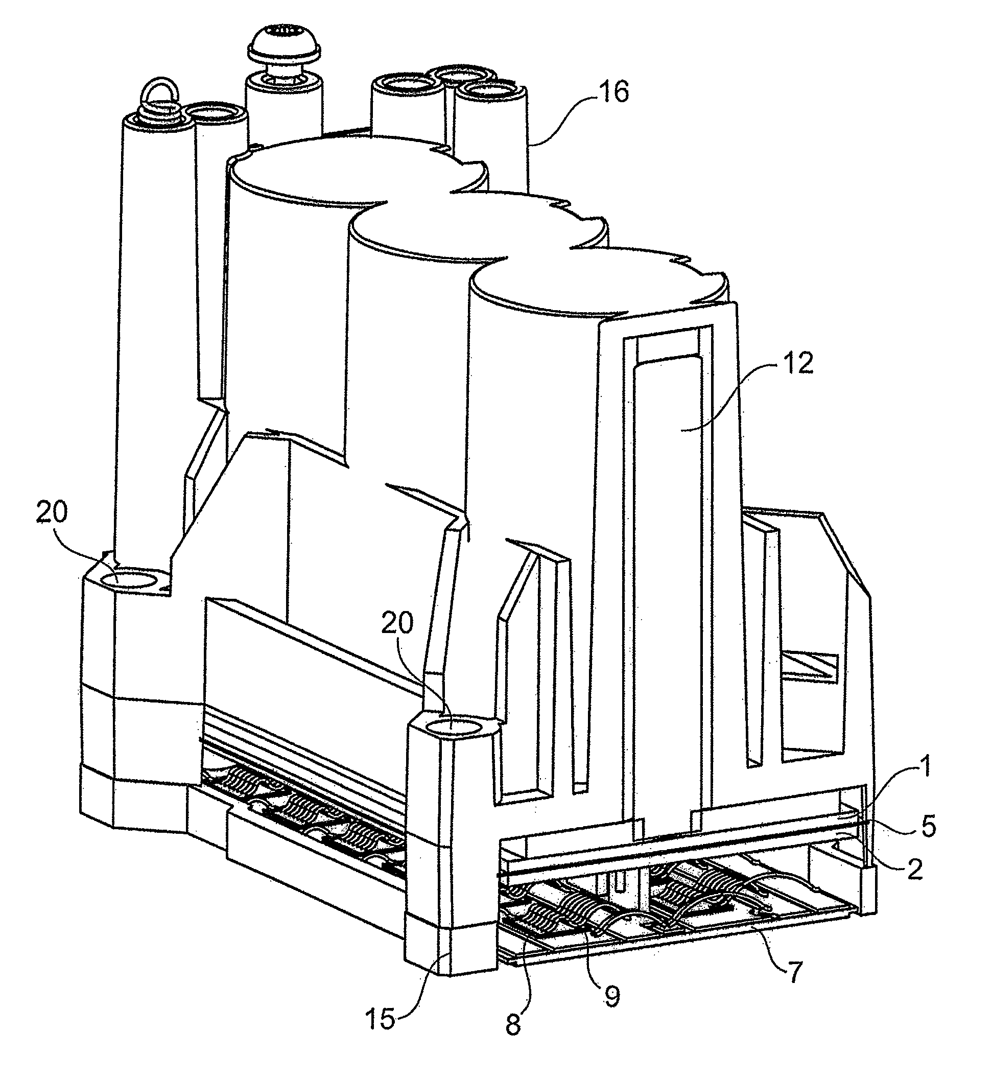
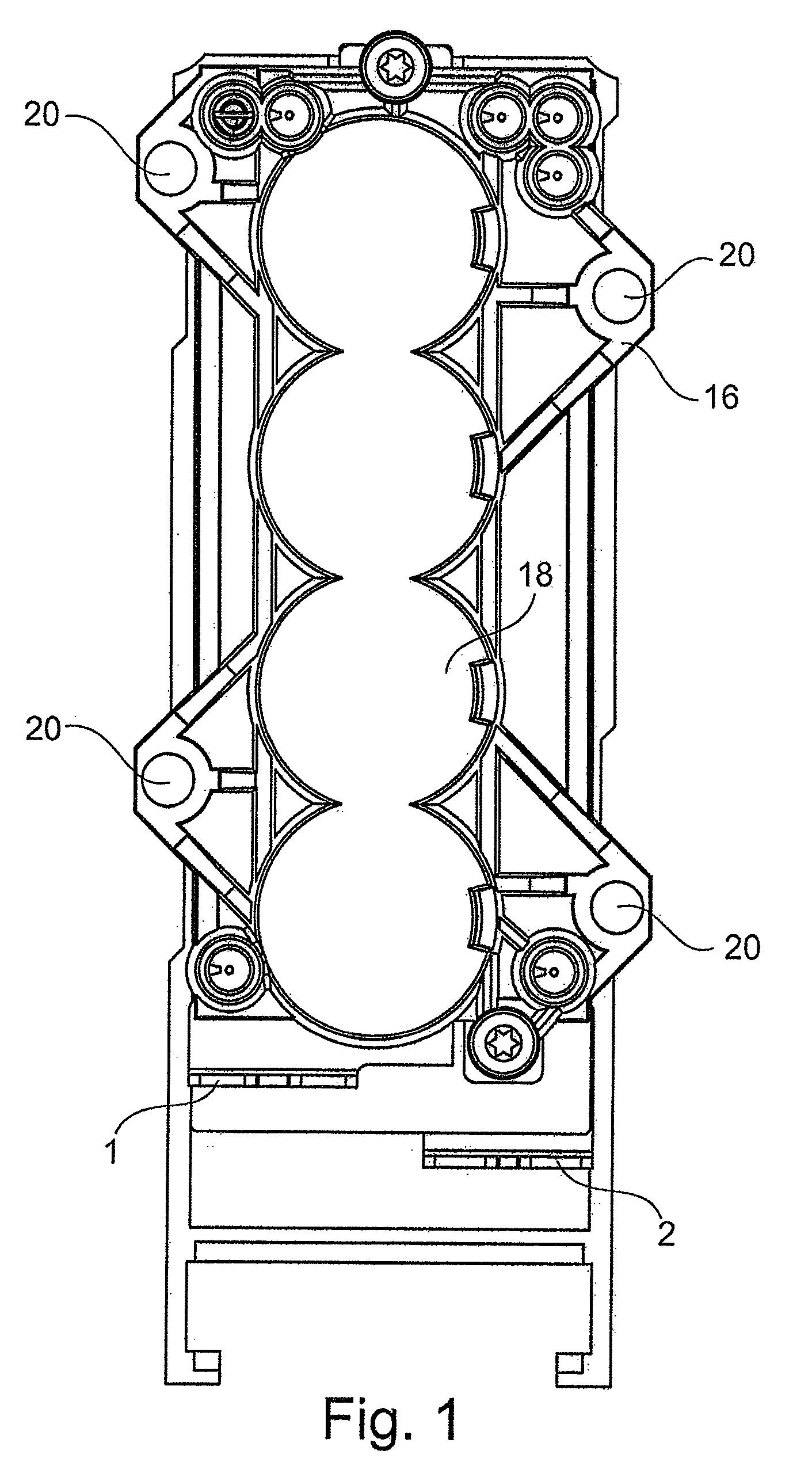
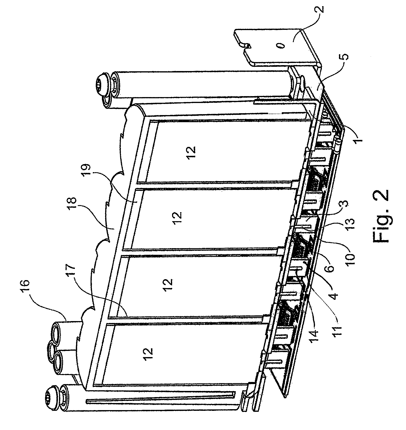
[0021]In the figures, a first load connection element is shown generally at 1 and a second load connection element is shown generally at 2. First and second load connection elements 1, 2 are in each case formed from a plate-type metal body having first contact feet 3 and second contact feet 4 extending therefrom. First and second load connection elements 1, 2 are stacked one above the other with an electrically insulating layer 5 disposed therebetween. Second load connection element 2 and electrically insulating layer 5 in each case have perforations 6 through which first contact feet 3 extend.

[0022]A substrate 7, produced using DCB technology, for example, accommodates power semiconductors 8 therein. Power semiconductors 8 are connected to first contact areas 10 and second contact areas 11 by means of bonding wires 9. The first and / or second contact areas 10, 11 may also be formed from a plurality of bonding wires 9 that are arranged alongside one another and bear on substrate 7. F...


PUM


Abstract

A power semiconductor module in which a substrate is provided with at least one power semiconductor and has first and second contact areas, wherein a first load connection element with first contact elements provided thereon is supported on the first contact areas and a second load connection element with second contact elements provided thereon is supported on the second contact areas. Wherein at least one spring element is provided for producing a pressure contact between the contact elements and the contact areas. To reduce the structural size of the module, the pressure contact between the contact elements and the contact areas is exerted by at least one electrical component arranged between the spring element and one of the load connection elements.

Description

BACKGROUND OF THE INVENTION[0001]1. Field of the Invention[0002]The invention relates to a power semiconductor module in which a substrate is provided with at least one power semiconductor and first and second contact areas.[0003]2. Description of the Related Art[0004]Such a power semiconductor module is known from U.S. Pat. No. 7,589,418. In the known power semiconductor module, a substrate having first and second contact areas is supported by its underside—i.e., the side facing away from the contact areas—on a heat sink. Power semiconductors are mounted on the opposite (top) side, the power semiconductors being electrically conductively connected to the contact areas. The contact areas serve, for example, for connection to a current source. For this purpose, load connection elements produced from metal sheets may be provided, with contact feet extending from the load connection elements. To produce an electrical contact, the load connection elements are supported by their contact ...

Claims


Application Information

Patent Timeline
Patent Type & Authority Patents(United States)
IPC IPC(8): H05K7/00
CPCH01L23/049H01L23/48H01L23/642H01L25/072H01L2924/12041H01L2924/01068H01L24/49H01L24/48H01L2224/48227H01L2224/49111H01L2924/01078H01L2924/19041H01L2924/00H01L2924/00014H01L2924/181H01L2224/45099H01L2224/45015H01L2924/207H01L23/04H01L24/72
Inventor FRANK, THOMAS
Owner SEMIKRON ELECTRONICS GMBH & CO KG
Why Eureka
Try Eureka