Method for producing cavities having optically transparent wall

a technology of optical transparency and production method, which is applied in the manufacture of cables/conductor parts, microstructural devices, liquid/fluent solid measurements, etc., can solve the problems of complex manufacturing method, high cost, and even more cost of method known from standard practice, and achieve high etching selectivity and high etching rate

Inactive Publication Date: 2009-01-20
ROBERT BOSCH GMBH
View PDF25 Cites 1 Cited by
  • Summary
  • Abstract
  • Description
  • Claims
  • Application Information

AI Technical Summary

Benefits of technology

[0004]The present invention proposes a method which will enable cavities having optically transparent walls to be produced simply and cost-effectively in a component by using standard methods of Microsystems technology. In this context, the method of the present invention also enables other functional elements to be integrated in the component.
[0006]The present invention has recognized that it is very simple to produce cavities having optically transparent walls by using Microsystems technology, when the walls act at the same time as an etch barrier layer, i.e., when a substance whose etching rate is high in relation to the silicon is used to dissolve out the silicon and which, at the same time, has a high etching selectivity with respect to the material of the cladding layer. Essential to the method of the present invention are, therefore, not only producing a silicon region which is surrounded on all sides by an optically transparent cladding layer, but also a suitable combination of cladding layer material and etching means. To dissolve out the silicon, the cladding layer may be advantageously opened at locations where access openings are provided for the cavity or channel—due to the component's function. Besides making it possible for a cavity having a transparent wall to be produced, the techniques used within the framework of the method of the present invention also enable other functional elements to be implemented, such as light-emitting regions having porous silicon, photodiodes, micromechanical elements, such as pumps and valves, a corresponding control or evaluation circuit, etc.
[0008]The silicon surrounded by the cladding layer may be dissolved out using wet-chemical etching or also vapor-phase etching. In the vapor phase, xenon difluoride XeF2 is advantageously used for the etching process, since it makes possible very high etching rates and substantial undercut etching of the cladding layer.

Problems solved by technology

On the whole, this method is very costly.
In this case, it turns out to be even more costly and complex to fabricate the component using the method known from standard practice.

Method used


Image

  • Method for producing cavities having optically transparent wall
  • Method for producing cavities having optically transparent wall
  • Method for producing cavities having optically transparent wall

Examples


Embodiment Construction

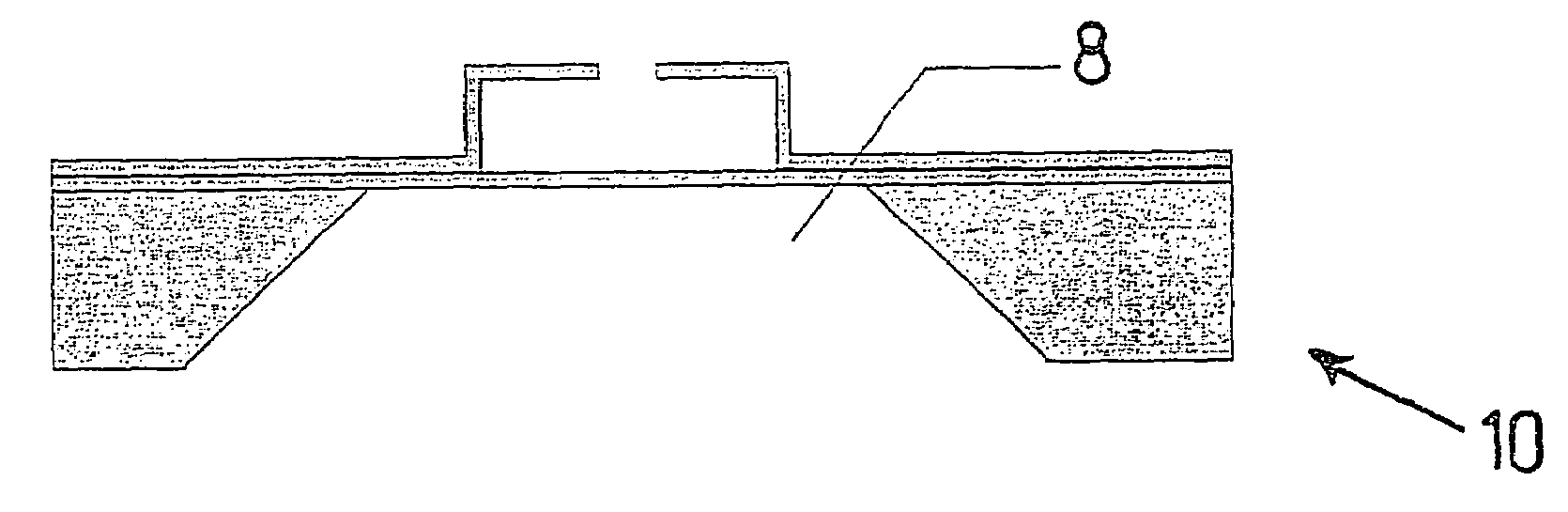
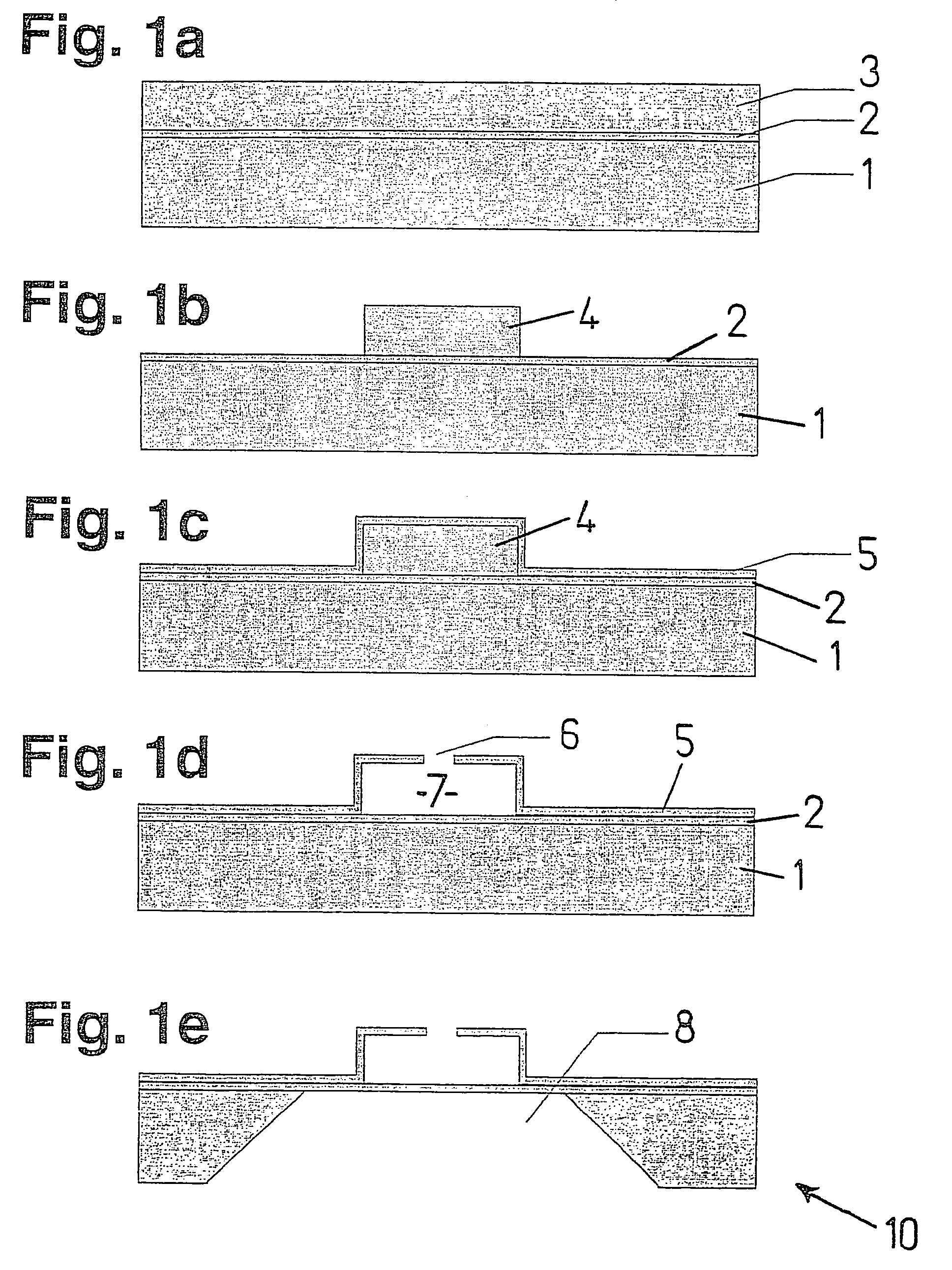
[0015]As just mentioned, FIGS. 1a through 1e show a component 10 in the individual phases of a variant of the method of the present invention for producing a cavity having an optically transparent wall. Here, component 10 is implemented on a silicon substrate 1. In the exemplary embodiment shown here, however, component 10 may also be implemented on another substrate that is suited for use in Microsystems technology.

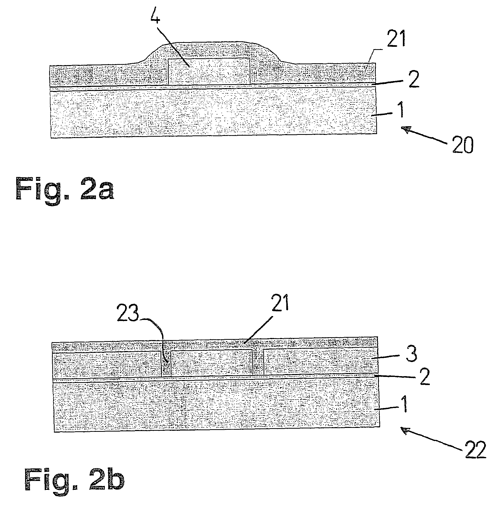
[0016]The layer construction shown in FIG. 1a corresponds to that of an SOI wafer, but may also be implemented by starting out from a silicon wafer that forms substrate 1. To this end, a silicon oxide layer 2 is produced on substrate 1. This may be accomplished by oxidation of silicon wafer 1 or also by deposition of silicon oxide onto the surface of silicon wafer 1. The silicon oxide layer is optically transparent. A polycrystalline silicon-epitaxy layer 3 is subsequently deposited onto silicon oxide layer 2.

[0017]At this point, silicon-epitaxy layer 3 is structured in ...


PUM

PropertyMeasurementUnit
transparentaaaaaaaaaa
optically transparentaaaaaaaaaa
electrical insulationaaaaaaaaaa

Abstract

A method is proposed which will enable cavities having optically transparent walls to be produced simply and cost-effectively in a component by using standard methods of microsystems technology. For this purpose, a silicon region is first produced, which is surrounded on all sides by at least one optically transparent cladding layer. At least one opening is then produced in the cladding layer. Over this opening, the silicon surrounded by the cladding layer is dissolved out, forming a cavity within the cladding layer. In this context, the cladding layer acts as an etch barrier layer.

Description

FIELD OF THE INVENTION[0001]The present invention is directed to a method for producing cavities having optically transparent walls in a component using Microsystems technology.BACKGROUND INFORMATION[0002]Components having such cavities are used, for example, in optical examinations of gases or liquids. Chemical reactions initiated by the action of light, for example a laser beam, can also be carried out in cavities having optically transparent walls. Components having optically transparent channels are also used for optical level checking.[0003]To fabricate components which have cavities and, in particular, channels having optically transparent walls, it is standard practice to bond one or more glass wafers to the substrate of the component. On the whole, this method is very costly. If the component is intended to be used in optical investigations of liquids or gases, glass fibers are often integrated in the component to enable light to be coupled into the cavity. In this case, it ...

Claims


Application Information

Patent Timeline
Patent Type & Authority Patents(United States)
IPC IPC(8): H01B13/00B81B1/00B81B3/00B81C1/00
CPCB81C1/00047B81C1/00246B81C2201/0115B81C2201/014
Inventor BENZEL, HUBERTWEBER, HERIBERTSCHAEFER, FRANK
Owner ROBERT BOSCH GMBH
Why Eureka
Try Eureka