Optoelectronic transmission device
a transmission device and optoelectronic technology, applied in the field of optoelectronic transmission devices, can solve problems such as poor optical transmittan
- Summary
- Abstract
- Description
- Claims
- Application Information
AI Technical Summary
Benefits of technology
Problems solved by technology
Method used
Image

Examples
Embodiment Construction
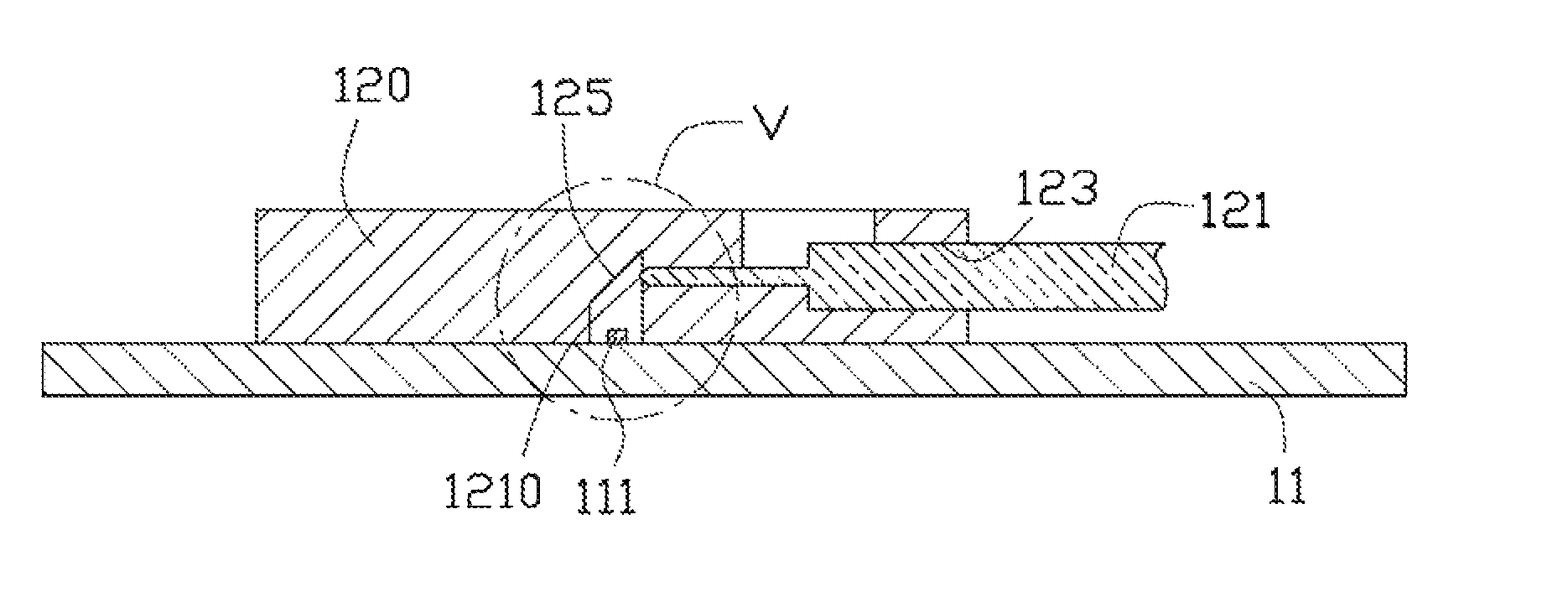
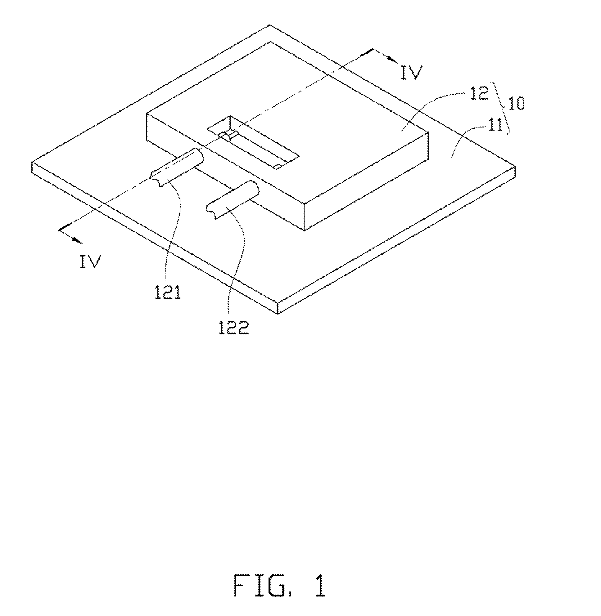
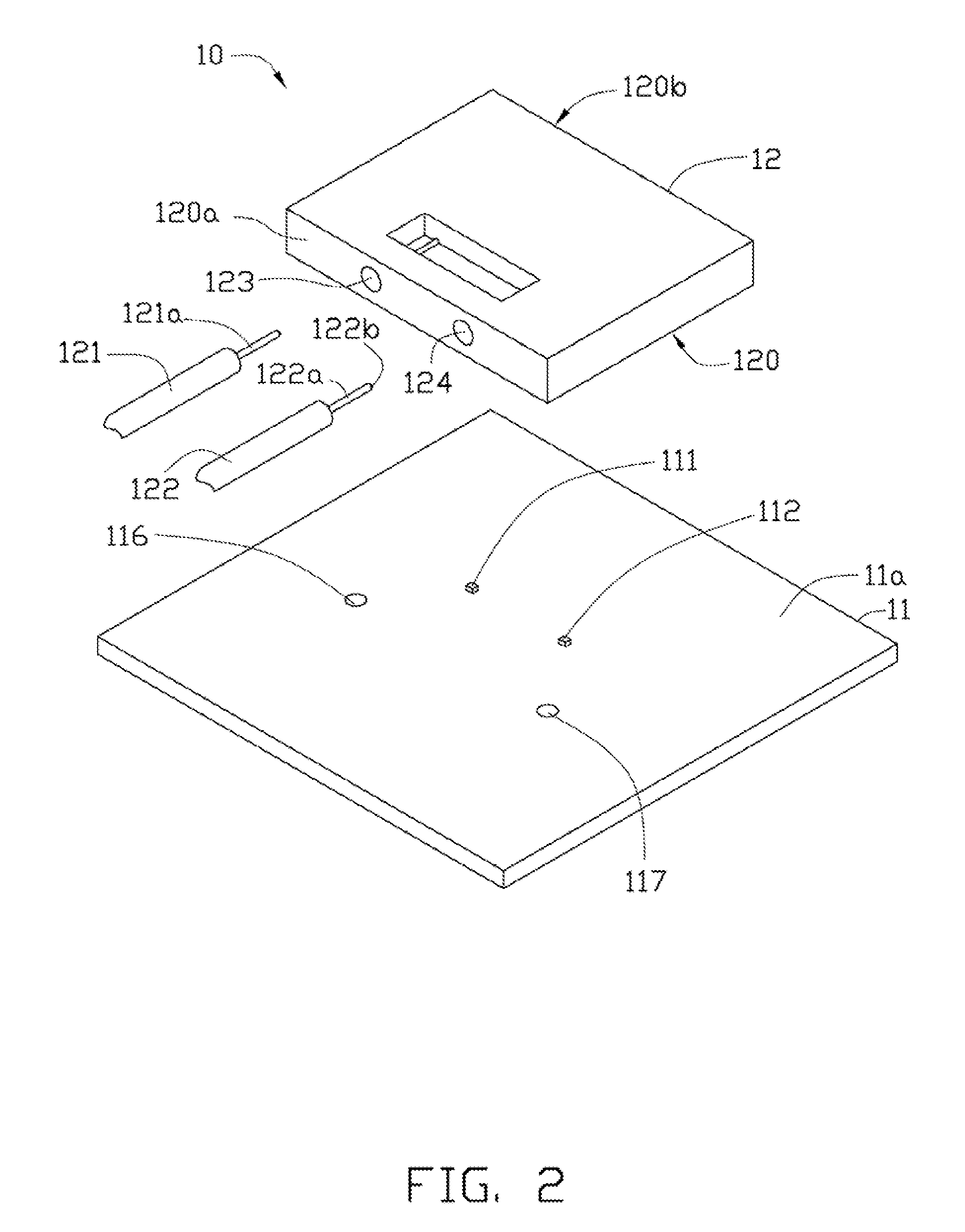
[0013]Referring to FIGS. 1 to 5, an optoelectronic transmission device 10, according to a first embodiment, includes a base 11, a carrier 12, an optical signal source 111, a light detector 112, and two lensed optical fibers 121, 122 (hereinafter a first lensed optical fiber 121 and a second lensed optical fiber 122).
[0014]The base 11 may be a printed circuit board. The optical signal source 111 and the light detector 112 are positioned on the base 11 and electrically connected to the base 11. The optical signal source 111 may be a laser diode and the light detector 112 may be a photodiode. A first positioning hole 116 and a second positioning hole 117 are defined in a surface 11a of the base 11 where the optical signal source 111 and the light detector 112 are positioned.
[0015]The carrier 12 is substantially a cuboid. The carrier 12 includes a bottom surface 120, a first side surface 120a and a second side surface 120b. The first side surface 120a and the second side surface 120b ar...
PUM
 Abstract
Description
Claims
Application Information