Wafer level camera module and method of manufacture

a technology of camera modules and wafers, applied in the field of digital cameras, can solve the problems of icds being vulnerable to damage and contamination, icds being vulnerable to contamination from particulate debris, and visible defects in images captured by the device, so as to facilitate higher yield and reduce manufacturing costs. , the effect of speeding up throughpu

Inactive Publication Date: 2013-06-04
NANCHANG O FILM OPTICAL ELECTRONICS TECH CO LTD
View PDF80 Cites 8 Cited by
  • Summary
  • Abstract
  • Description
  • Claims
  • Application Information

AI Technical Summary

Benefits of technology

[0009]Embodiments of the present invention overcome problems associated with the prior art, by providing a digital camera module with lenses formed at the wafer level. Embodiments of the present invention facilitate higher yield, faster throughput, and lower manufacturing costs by eliminating the need to attach a lens assembly within a housing. In some embodiments, quality may improve due to less handling and fewer materials. Also, because the module is fabricated at the wafer level, clean room technology may be employed to reduce the risk of ICD damage or contamination. Further, in some embodiments, the overall size of the digital camera module may be reduced in all three dimensions.
[0010]In accordance with an embodiment, the present invention provides a digital camera module comprising an ICD including an imager; a first transparent element; a bonding agent coupling said ICD to said first transparent element without blocking incident light to said imager; and a second transparent element coupled to said first transparent element. In one embodiment, no portion of said first transparent element and said second transparent element extends beyond the perimeter of the ICD. The first transparent element may include a concave-convex section and said second transparent element may include a convex-concave section. The bonding agent may include a die-cut adhesive sheet and / or dispensed adhesive. The adhesive sheet and / or the dispensed adhesive may include opaque material and / or waterproof material. The first transparent element and the second transparent element may form an airgap therebetween, and said first transparent element and said ICD may form an airgap therebetween. The second transparent element may be coupled to said first transparent element via a bonding agent. The second transparent element may be coupled to said first transparent element via mechanical interaction. The mechanical interaction may include complementary interlocking features formed on said first transparent element and said second transparent element. Additional transparent elements can be added to further improve image quality.
[0011]In accordance with another embodiment, the present invention provides a digital camera module workpiece, comprising an ICD wafer including an array of ICDs; a first transparent element array including an array of first transparent elements, each first transparent element positioned over a respective one of said ICDs; and a second transparent element array including an array of second transparent elements, each second transparent element positioned over a respective one of said first transparent elements. In one embodiment, the perimeter of each first transparent element and its respective second transparent element does not extend beyond the perimeter of its respective ICD. The workpiece may further comprise metallization coupled to the ICD. The first transparent element array may be coupled to said ICD wafer via a bonding agent. The ICD wafer and first transparent element array may be backlapped. The ICD wafer may be plasma etched on the side opposite said first transparent element array to form holes for accessing bonding pads. These holes are then metallized to reposition electrical contacts on the bottom surface of the ICD, where solder balls can be attached to form a wafer level package. The second transparent element array may be coupled to said first transparent element array via a bonding agent. The second transparent element array may be coupled to said first transparent element array via mechanical interactions. The mechanical interactions may include complementary interlocking features formed on said first transparent elements and said second transparent elements. Additional interlocking transparent elements may be added to further improve image quality.

Problems solved by technology

Further, camera module and host device manufacturers want the incorporation of the camera modules into the host devices not to compromise image quality.
ICDs are vulnerable to damage and contamination, particularly before and during the housing attachment process.
For example, before the housing is attached to the PCB, the wire bonds are exposed to inadvertent contact (e.g., during handling), which can cause damage.
Further, the ICD is vulnerable to contamination from particulate debris.
Contamination of the sensor array (the image capture surface) may block incident light, causing visible defects in images being captured by the device.
Damaged ICDs may cause a decrease in product yield and an increase in labor and material costs.

Method used


Image

  • Wafer level camera module and method of manufacture
  • Wafer level camera module and method of manufacture
  • Wafer level camera module and method of manufacture

Examples


Embodiment Construction

[0021]In the following description, numerous details are set forth to provide a thorough understanding of the present invention. Those skilled in the art will recognize that the present invention may depart from these details. Further, details of well-known practices and components have been omitted, so as not to unnecessarily obscure the present invention.

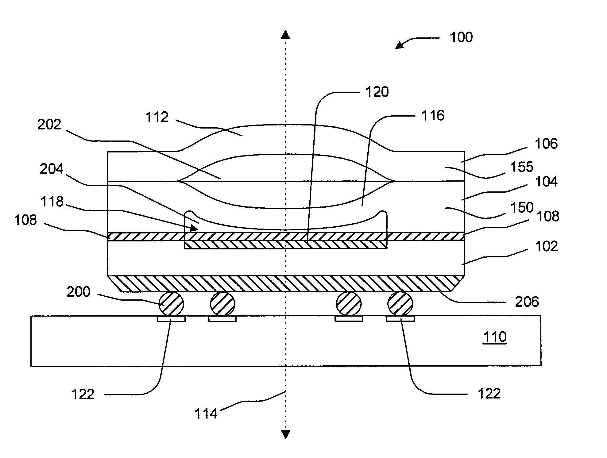
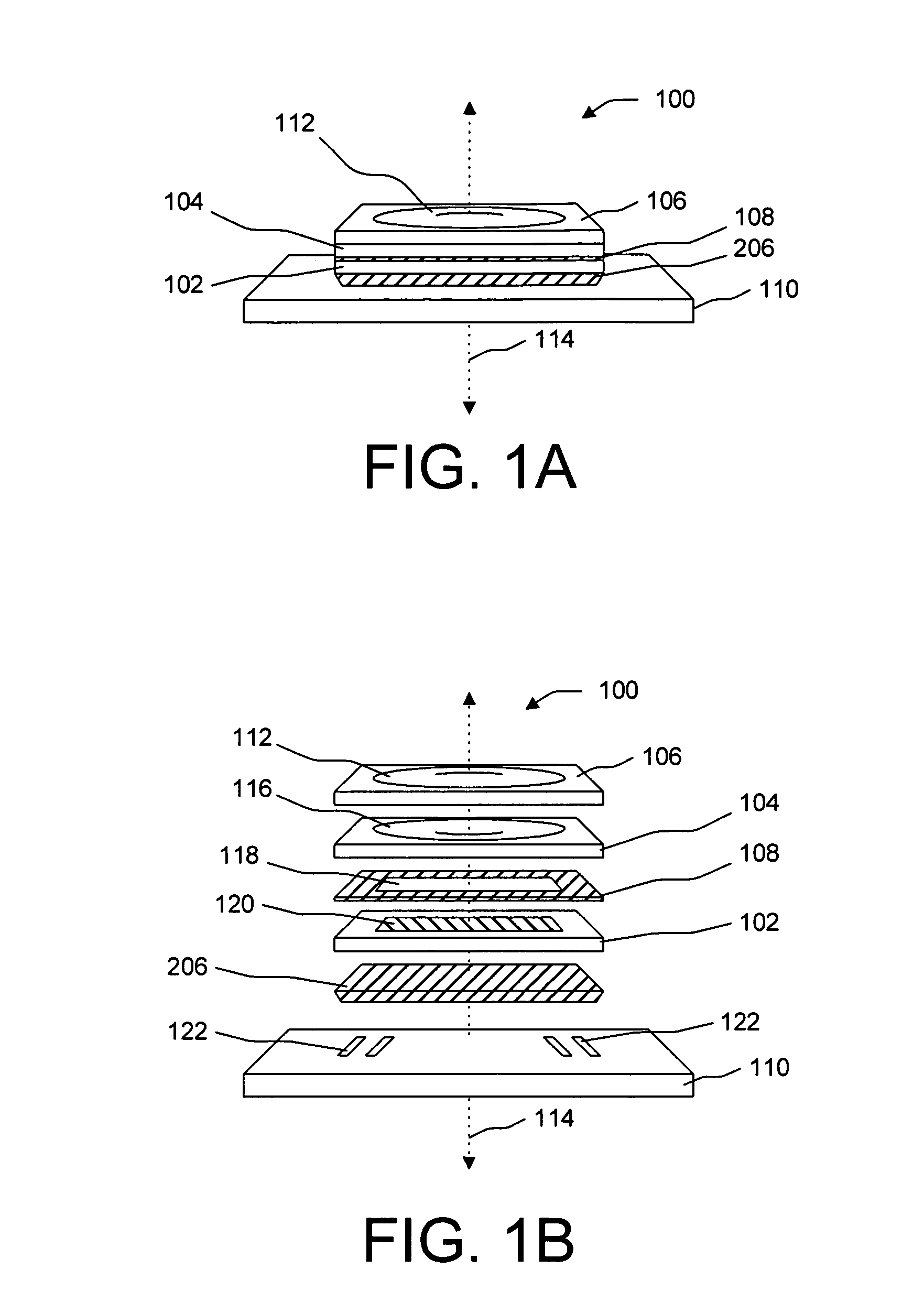
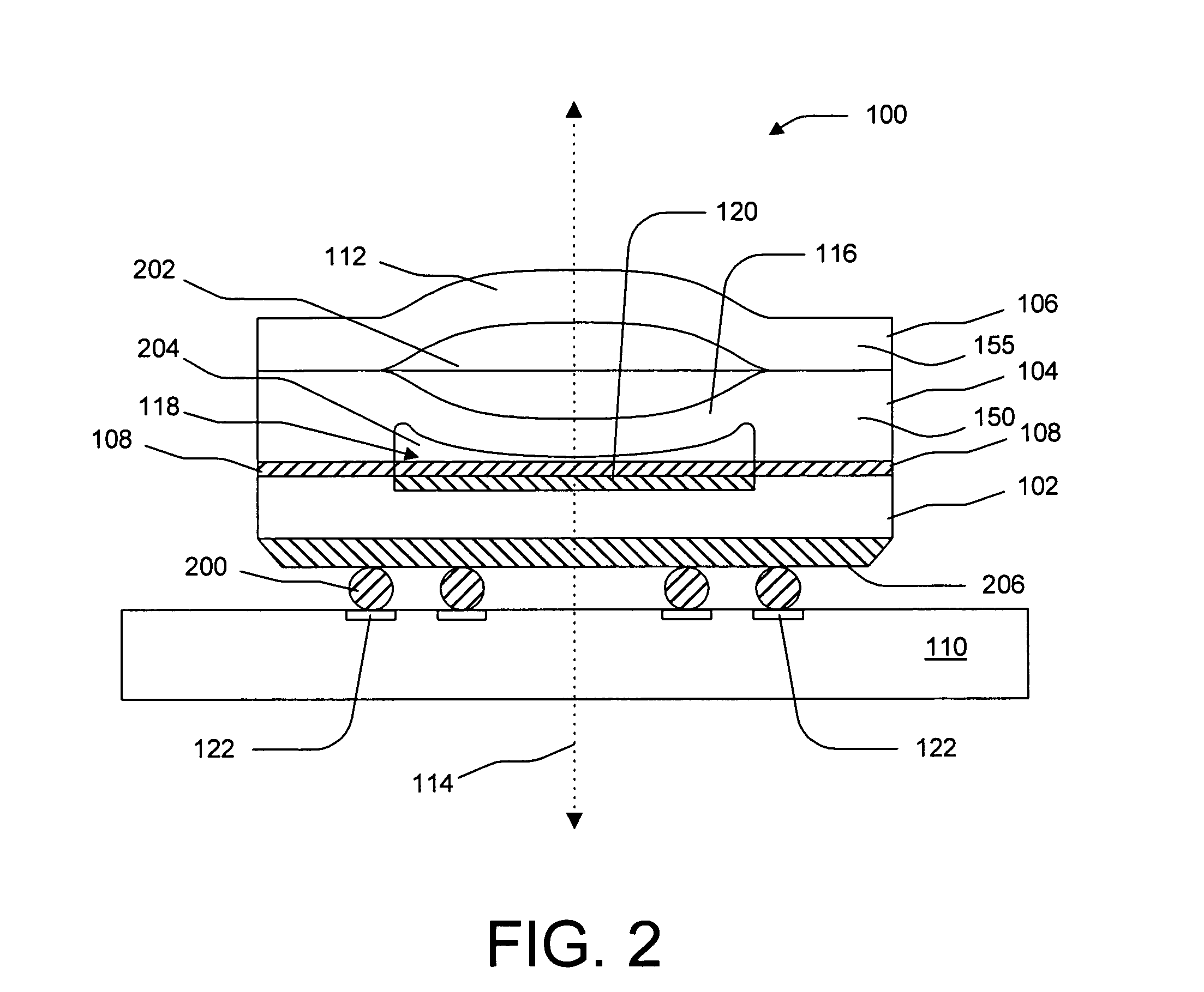
[0022]Embodiments of the present invention overcome problems associated with the prior art, by providing a digital camera module with lenses formed thereon at the wafer level. Embodiments of the present invention facilitate higher yield, faster throughput, and lower manufacturing costs by eliminating the need to attach the lens assembly within a housing. In some embodiments, quality may improve due to less handling and fewer materials. Also, because the module is fabricated at the wafer level, clean room technology may be employed to reduce the risk of ICD damage and / or contamination. Further, in some embodiments, the overall size...


PUM

PropertyMeasurementUnit
transparentaaaaaaaaaa
perimeteraaaaaaaaaa
waterproofaaaaaaaaaa

Abstract

A method includes forming optical lenses on an ICD at the wafer level, rather than attaching a separate lens assembly. The lenses may be formed as an array of individual lenses or as multiple, e.g., two, arrays of individual lenses. The array of lenses may be coupled to an array of ICDs. The ICDs and individual lenses in the array assembly may be singulated to form individual digital camera modules. Additionally or alternatively, the ICDs and individual lenses may be singulated in separate steps.

Description

BACKGROUND[0001]1. Technical Field[0002]This invention relates generally to digital cameras, and more particularly to digital camera modules mountable in host devices.[0003]2. Description of the Background Art[0004]Digital camera modules are currently being incorporated into a variety of host devices. Such host devices include cellular telephones, personal data assistants (PDAs), computers, etc. And, consumer demand for digital camera modules in host devices continues to grow.[0005]Host device manufacturers prefer digital camera module to be small, so that they can be incorporated into the host device without increasing the overall size of the host device. Further, host device manufacturers desire camera modules that minimally affect host device design. Further, camera module and host device manufacturers want the incorporation of the camera modules into the host devices not to compromise image quality.[0006]A conventional digital camera module generally includes a lens assembly, a ...

Claims


Application Information

Patent Timeline
Patent Type & Authority Patents(United States)
IPC IPC(8): G02B13/16H04N5/225H01L31/0203
CPCH01L27/14625H01L27/14627H04N5/2254H01L27/14685Y10T29/49128H04N23/55H04N25/41
Inventor SINGH, HARPUNEET
Owner NANCHANG O FILM OPTICAL ELECTRONICS TECH CO LTD
Why Eureka
Try Eureka