Display device
a technology of a display device and a connector is applied in the field of display devices, which can solve the problems of affecting the repair effect of the line, the repair is not possible, and so as to achieve the effect of repairing the disconnection of the line in the wiring
- Summary
- Abstract
- Description
- Claims
- Application Information
AI Technical Summary
Benefits of technology
Problems solved by technology
Method used
Image

Examples
first embodiment
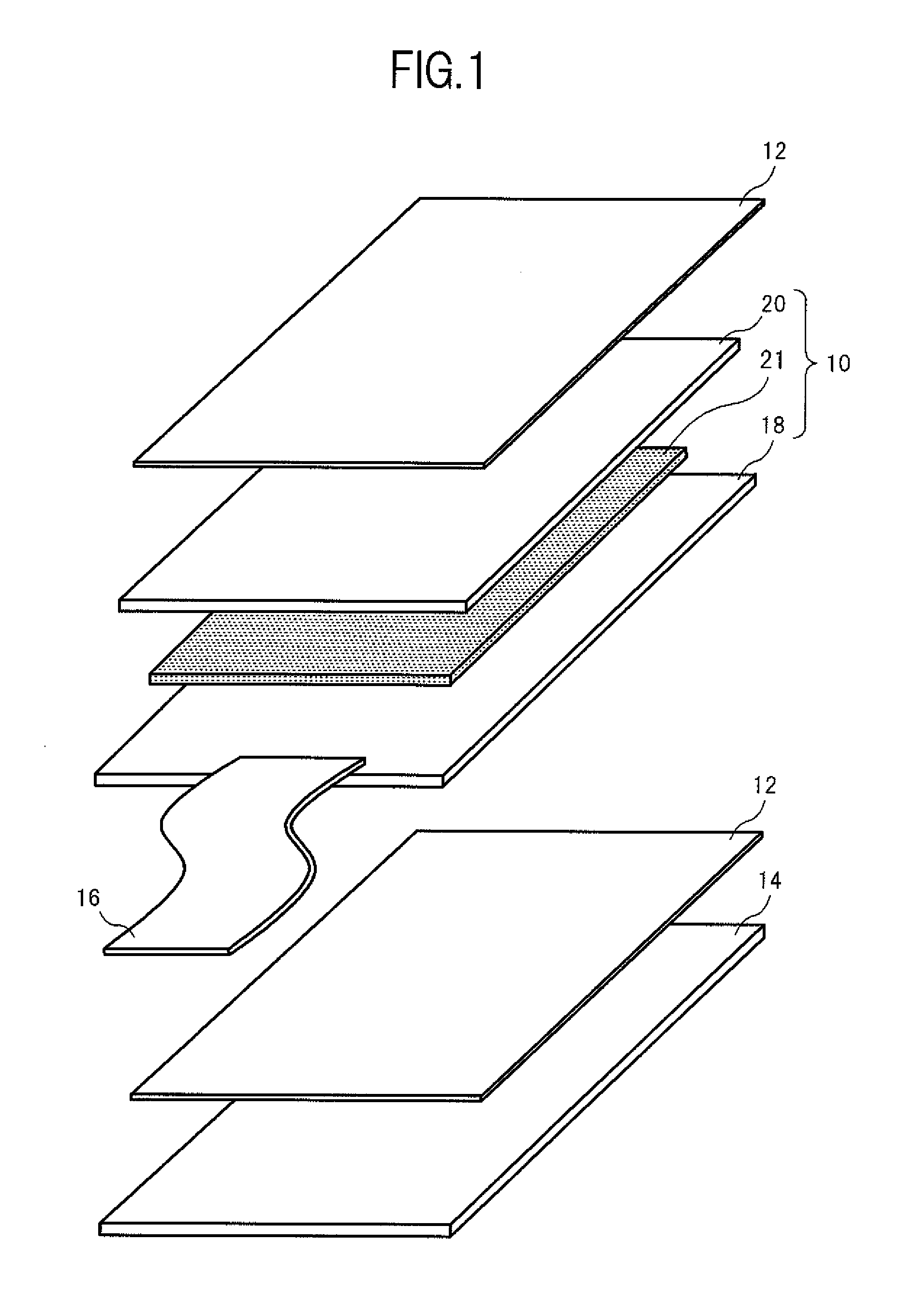
[0040]FIG. 1 is an exploded perspective view showing a display device according to a first embodiment of the present invention. The explanation of the display device is made hereinafter by taking a liquid crystal display device as an example. The liquid crystal display device includes a liquid crystal panel 10. A polarizer 12 is arranged on both surfaces of the liquid crystal panel 10 respectively. The liquid crystal display device includes a backlight 14. One polarizer 12 is interposed between the liquid crystal panel 10 and the backlight 14. A flexible printed circuit board 16 is mounted on the liquid crystal panel 10.
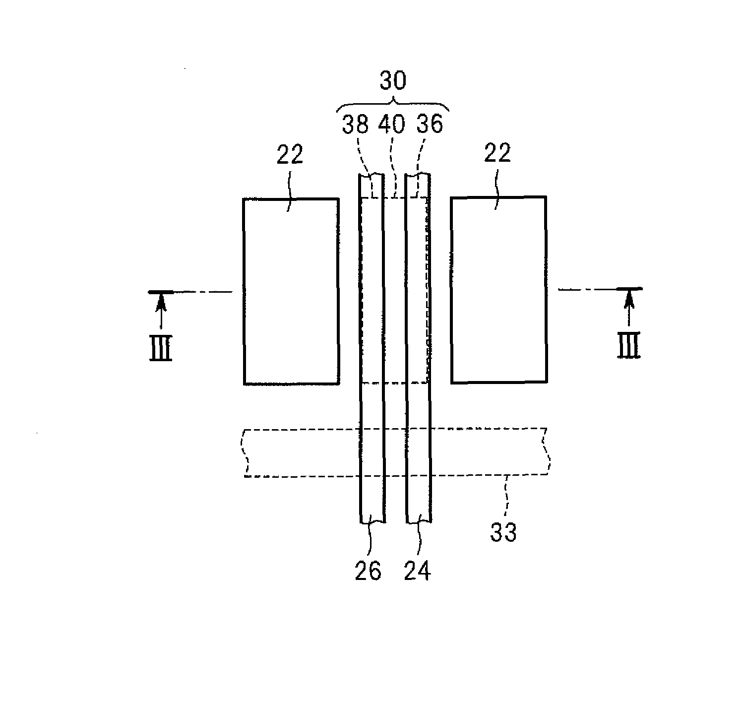
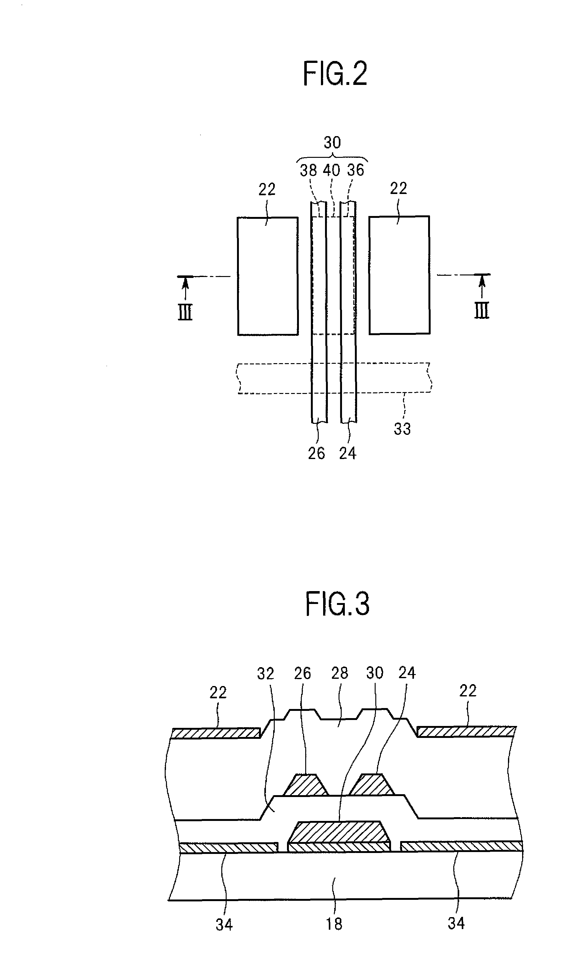
[0041]The liquid crystal panel 10 includes a substrate 18 and a counter substrate 20 which faces the substrate 18 in an opposed manner, and liquid crystal 21 is interposed between both substrates. The substrate 18 is a TFT (Thin Film Transistor) substrate (or an array substrate) which includes thin-film field effect transistors, pixel electrodes, lines and the like. ...
second embodiment
[0057]FIG. 10 is a plan view showing a portion of the display device according to a second embodiment in an enlarged manner.
[0058]In this embodiment, a connecting portion 140 of a conductive layer 130 includes a first connecting portion 141 and a second connecting portion 142 which are arranged in a spaced-apart manner from each other. Further, the conductive layer 130 includes a slit 144 in a region which is surrounded by a first overlapping portion 136, a second overlapping portion 138, the first connecting portion 141 and the second connecting portion 142. In other words, the conductive layer 130 has a blanked square shape. Other constitutions of this embodiment correspond to the corresponding constitutions explained in conjunction with the first embodiment.
[0059]According to this embodiment, the slit 144 formed in the conductive layer 130 is arranged between a first line 24 and a second line 26. Accordingly, even when the first line 24, the second line 26 and the conductive laye...
third embodiment
[0065]FIG. 16 is a plan view showing a portion of a display device according to a third embodiment in an enlarged manner.
[0066]In this embodiment, a first overlapping portion 236 of a conductive layer 230 which overlaps with a first line 24 includes a pair of first portions 246 which is arranged in a spaced-apart manner from each other. Further, a second overlapping portion 238 of the conductive layer 230 which overlaps with a second line 26 includes a pair of second portions 248 which is arranged in a spaced-apart manner from each other. Further, one first portion 246 and one second portion 248 are arranged adjacent to each other, and another first portion 246 and another second portion 248 are arranged adjacent to each other.
[0067]A connecting portion 240 includes a first connecting portion 241 which extends between one first portion 246 and one second portion 248 arranged adjacent to each other, a second connecting portion 242 which extends between another first portion 246 and a...
PUM
| Property | Measurement | Unit |
|---|---|---|
| conductive | aaaaa | aaaaa |
| width | aaaaa | aaaaa |
| distance | aaaaa | aaaaa |
Abstract
Description
Claims
Application Information
 - R&D
- Intellectual Property
- Life Sciences
- Materials
- Tech Scout
- Unparalleled Data Quality
- Higher Quality Content
- 60% Fewer Hallucinations
Browse by: Latest US Patents, China's latest patents, Technical Efficacy Thesaurus, Application Domain, Technology Topic, Popular Technical Reports.
© 2025 PatSnap. All rights reserved.Legal|Privacy policy|Modern Slavery Act Transparency Statement|Sitemap|About US| Contact US: help@patsnap.com