
Package structure enhancing molding compound bondability

a technology of packaging structure and molding compound, which is applied in the direction of electrical equipment, semiconductor devices, semiconductor/solid-state device details, etc., can solve the problems of easy delamination and serious affecting product yield during a manufacturing process, and achieve the effect of enhancing the bondability between the leadframe and the molding compound and reducing the loading stress

Inactive Publication Date: 2013-07-02
KUN YUAN TECH
View PDF5 Cites 0 Cited by
  • Summary
  • Abstract
  • Description
  • Claims
  • Application Information

AI Technical Summary

Benefits of technology

Significantly improves the bondability between the leadframe and molding compound, reducing delamination risks and enhancing manufacturing yield while allowing for optimal adjustment of graspability and holdability during the manufacturing process.

Problems solved by technology

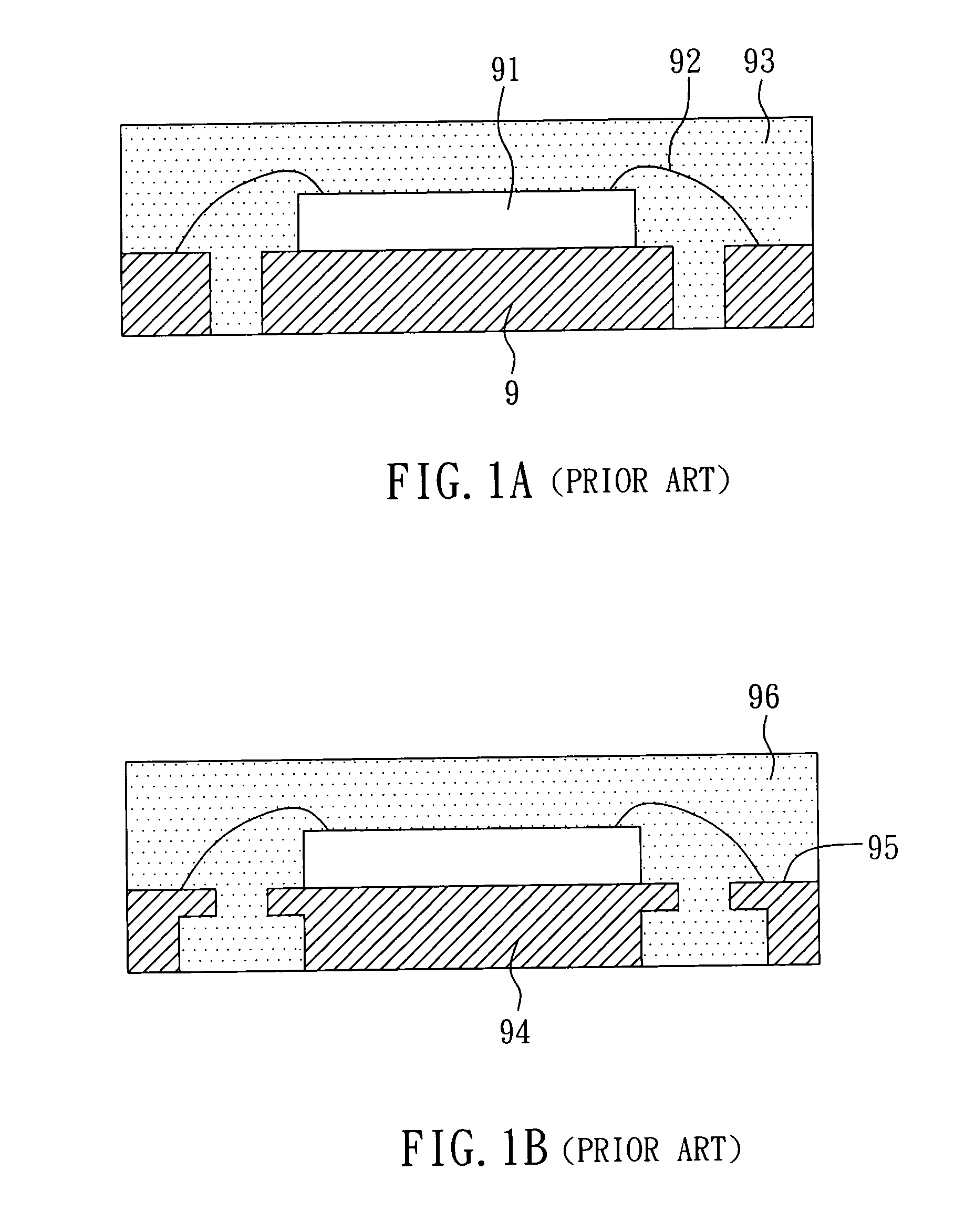
This will worsen delamination between the leadframe 9 and the molding compound 93, or even result in singulation which causes detachment of leads, seriously affecting the product yield during a manufacturing process.
Nevertheless, in spite of the fact that this measure may somewhat improve the bondability, such improvement is considered insufficient, and the situation of delamination can still take place easily.

Method used


Image

  • Package structure enhancing molding compound bondability
  • Package structure enhancing molding compound bondability
  • Package structure enhancing molding compound bondability

Examples


Embodiment Construction

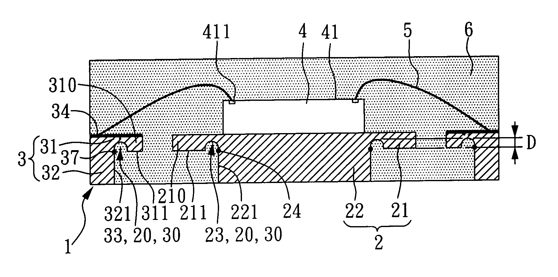
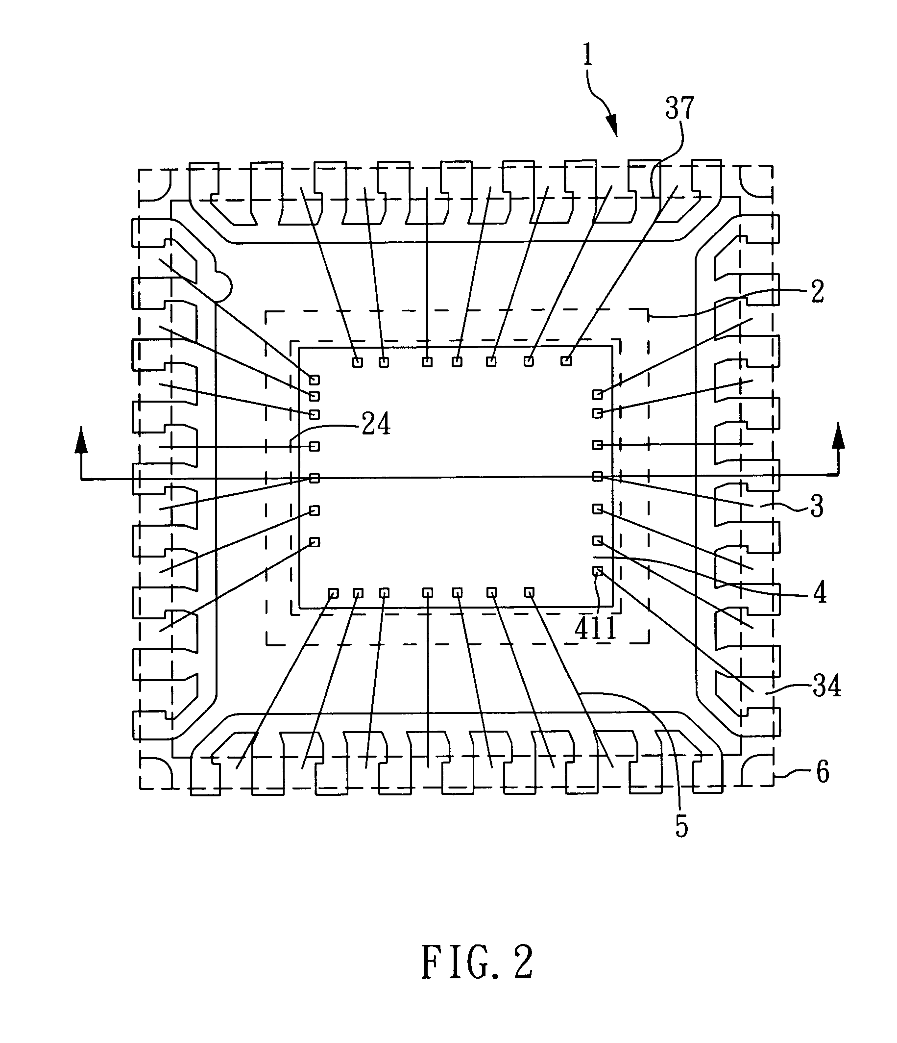
[0026]Referring to FIG. 2, a top view illustrating a package structure enhancing molding compound bondability according to a first embodiment of the present invention, to FIG. 3A, a cross-sectional view taken from FIG. 2, and to FIG. 3B, an enlarged cross-sectional view illustrating part of the package structure as shown in FIG. 3A, the package structure comprises primarily a leadframe 1, a chip 4, a plurality of wires 5, and a molding compound 6.

[0027]According to the present invention, the leadframe 1 includes a chip base 2 and a pin holder 3, wherein the chip base 2 includes a chip pad 21 and a support 22. The chip pad 21 is integrally connected with an upper portion of the support 22, wherein a side protrusion 210 extends sideward from a sidewall 221 of the support 22, and the side protrusion 210 has a lower surface 211. Further, the lower surface 211 and the sidewall 221 interconnect at an intersection line 24, namely, the lower surface 211 and the sidewall 221 are connected at...


PUM


Abstract

A leadframe enhancing molding compound bondability includes a chip base and a pin holder. The chip bases includes a chip pad and a support, wherein the chip pad includes a side protrusion extending out of the support, and the side protrusion has a lower surface, and the support has a sidewall, and wherein the lower surface and the sidewall interconnect at an intersection line, and the lower surface is formed upwardly with a recess. Further, a pin holder includes a pin stand and a seat, wherein the pin stand has an edge portion extending out of the seat, the edge portion has a lower surface, the seat has a sidewall, and the lower surface and the sidewall interconnect at a crossing line. The lower surface of the pin stand is formed upward with a recess. As such, the bondability between the leadframe and the molding compound can be greatly enhanced.

Description

BACKGROUND OF THE INVENTION[0001]1. Field of the Invention[0002]The present invention relates to a leadframe enhancing molding compound bondability and a package structure thereof, and more particularly, to a leadframe for enhancing bondability with the molding compound encapsulating a semiconductor package, and to a structure of the semiconductor package.[0003]2. Description of Related Art[0004]Referring to FIG. 1A, a cross-sectional view illustrating a conventional semiconductor package, a semiconductor chip 91 is fixed on a conventional leadframe 9, where the semiconductor chip 91 is electrically connected with the leadframe 9 through gold wires 92. The semiconductor chip 91, the gold wires 92, and the leadframe 9 are encapsulated by molding compound 93 such that the purpose of protection and insulation can be achieved. However, along with continuous development of technology, electronic components have been developed rapidly toward the tendency of light, thin, short, and small. ...

Claims


Application Information

Patent Timeline
Patent Type & Authority Patents(United States)
IPC IPC(8): H01L23/13
CPCH01L23/3107H01L23/3142H01L23/49503H01L23/49548H01L23/49582H01L24/49H01L24/48H01L2924/01079H01L2224/85439H01L2224/85416H01L2224/49171H01L24/45H01L2224/45144H01L2224/48091H01L2224/48247H01L2924/00014H01L2924/00H01L2224/48616H01L2224/48639H01L2924/181H01L2224/05554H01L2924/18301H01L2924/00012
Inventor HSIA, CHENG-YUYEH, CHIAO-JUNG
Owner KUN YUAN TECH
Learn More