Stacked interposer leadframes

a leadframe and interposer technology, applied in the direction of semiconductor devices, electrical equipment, semiconductor/solid-state device details, etc., can solve the problems of small size of silicon chips on which integrated circuits are formed, sensitive to damage, and difficult to handle, so as to achieve the effect of minimal package size and improved heat dissipation

Active Publication Date: 2013-07-23
ANALOG DEVICES INT UNLTD
View PDF34 Cites 6 Cited by
  • Summary
  • Abstract
  • Description
  • Claims
  • Application Information

AI Technical Summary

Problems solved by technology

The silicon chips on which integrated circuits are formed are so small that they are sensitive to damage and hard to handle, and many IC chips are packaged in enclosures that protect the chips and provide larger contact leads that can be attached to circuitry on substrates such as printed circuit boards.
One approach to keeping the size of the integrated package down has been to stack IC chips, which presents challenges in providing interconnects and heat dissipation.

Method used


Image

  • Stacked interposer leadframes
  • Stacked interposer leadframes
  • Stacked interposer leadframes

Examples


Embodiment Construction

[0024]The system and method disclosed herein describe how multiple stacking leadframes are integrated with multiple IC die to form a stacked leadframe assembly that can be handled as an assembly in the process of packaging IC assemblies or can be integrated onto a substrate as part of an integrated assembly forming a more complicated single device.

[0025]In the following detailed description, numerous specific details are set forth to provide a full understanding of the present disclosure. It will be apparent, however, to one ordinarily skilled in the art that embodiments of the present disclosure may be practiced without some of the specific details. In other instances, well-known structures and techniques have not been shown in detail so as not to obscure the disclosure.

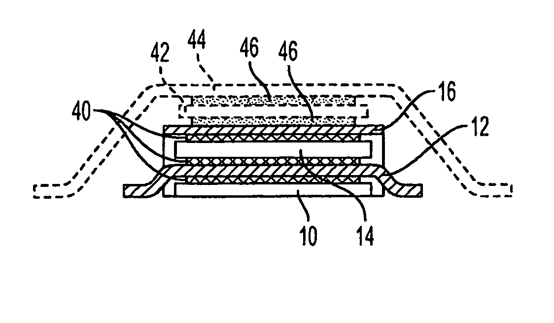
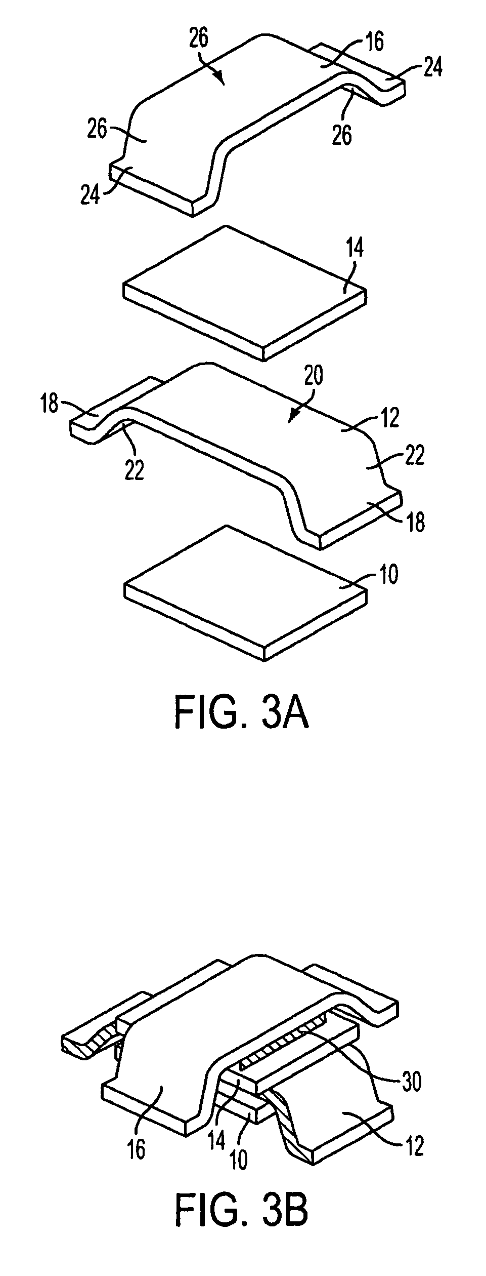
[0026]FIG. 3A is an exploded view of an embodiment of a leadframe stack assembly according to certain aspects of the present disclosure. Working upwards from the bottom of the stack, an IC die 10 is overlaid with a ...


PUM


Abstract

A stacked leadframe assembly is disclosed. The stacked leadframe assembly includes a first die having a surface that defines a mounting plane, a first leadframe stacked over and attached to the first die, a second die stacked over and attached to the first leadframe; and a second leadframe stacked over and attached to the second die. The leadframes have die paddles with extended side panels that have attachment surfaces in the mounting plane.

Description

BACKGROUND[0001]1. Field[0002]The present disclosure generally relates to integrated circuit (IC) packages and, more particularly, to leadframes and method of manufacturing leadframes for use in IC packages.[0003]2. Description of the Related Art[0004]The silicon chips on which integrated circuits are formed are so small that they are sensitive to damage and hard to handle, and many IC chips are packaged in enclosures that protect the chips and provide larger contact leads that can be attached to circuitry on substrates such as printed circuit boards. One common method of assembling an IC package of this type is to attach a “leadframe”, or “lead frame”, as a mechanical support to the die during its assembly. A portion of the leadframe is trimmed off, leaving only the leads that provide the external connections for the finished product. A leadframe comprises a “die paddle”, to which the die is attached, and “leads”, which provide external electrical connections. One method of connect...

Claims


Application Information

Patent Timeline
Patent Type & Authority Patents(United States)
IPC IPC(8): H01L23/495
CPCH01L23/49562H01L23/492H01L23/495H01L23/49537H01L21/50H01L2224/33181H01L2224/32245H01L2924/10253H01L2924/00
Inventor PRUITT, DAVID ALAN
Owner ANALOG DEVICES INT UNLTD
Why Eureka
Try Eureka