Printing semiconductor elements by shear-assisted elastomeric stamp transfer

a technology of elastomeric stamps and semiconductor elements, which is applied in the direction of dough shaping, manufacturing tools, applications, etc., can solve the problems of low energy required to initiate delamination of the transfer stamp surface, and achieve faster and more reliable transfer printing, sacrificing printing yield or accuracy, and high delamination rate

Active Publication Date: 2013-08-13
X DISPLAY CO TECH LTD
View PDF75 Cites 362 Cited by
  • Summary
  • Abstract
  • Description
  • Claims
  • Application Information

AI Technical Summary

Benefits of technology

[0007]Provided are methods and systems for dry transfer printing of semiconductors and semiconductor elements by shear offset. Shear offset printing systems permit higher delamination rates to be achieved during transfer printing without sacrificing printing yield or accuracy, compared to conventional techniques that do not apply a shear offset. Accordingly, methods and systems presented herein provide faster and more reliable transfer printing, thereby reducing processing time and increasing printing efficiency.
[0013]In an embodiment, any of the stamps used in any of the processes or devices disclosed herein may be a composite stamp. In an aspect, the elastomeric stamp has an elastomeric layer with a top surface that is opposite the transfer surface and a rigid backing layer having a bottom surface, wherein the bottom surface is positioned adjacent to the elastomeric layer top surface. Such elastomeric stamps having a rigid backing layer are advantageous for transferring applied pressure and motion (e.g., vertical and / or horizontal) to the interface between the transfer surface and the inked semiconductor element and / or the receiving substrate surface. For example, air pressure applied to the rigid backing can be uniformly transmitted to the active printing area. In another aspect, the elastomeric stamp also has a reinforcement layer operably connected to the rigid backing layer, the reinforcement layer having an opening that vertically coincides with at least a portion of the relief features on the transfer surface.
[0017]In an embodiment the relief features comprise a plurality of posts. The posts can help facilitate semiconductor element lift-off from a donor surface and / or semiconductor element transfer from the stamp to the receiving surface. In an aspect of this embodiment, the plurality of posts have a contacting area fraction on the transfer surface selected from a range that is greater than 1% and less than 25%. “Contacting area fraction” refers to the percentage of surface area coverage by the posts over the printable surface area region. In an aspect where the relief features comprise a plurality of populations, the relief features may further comprise a plurality of stabilization features interspersed between the posts, wherein said stabilization features have a contacting area that is less than the contacting area of the posts.
[0023]For aspects where air pressure is applied to at least partially establish said conformal contact and the stamp is vertically separated from the receiving surface, each of the air pressure and vertical separation rate may vary over time during the delamination cycle. For example, in embodiments where the delamination cycle is divided into at least two time intervals, with the first interval is before the second interval, and does not substantially overlap, the air pressure may vary over the first time interval while the vertical separation is maintained constant over this first time interval. In contrast, during the second time interval the air pressure may be maintained constant while the vertical separation increases during this second time interval. In this embodiment, selection of the pressure and separation distance with respect to time is an optimization step that helps facilitate a constant delamination rate over the delamination cycle, such a delamination rate that deviates less than or equal to a user-specified deviation, such as less than or equal to 5% from an average delamination rate over the first and second time intervals.
[0025]In an embodiment, the device supports a reinforced composite stamp having a deformable layer with an internal surface and an external surface positioned opposite the internal surface, the external surface of the deformable layer having a plurality of relief features. A rigid support layer is connected to the internal surface of the deformable layer, wherein the rigid support layer has a bottom surface and a top surface positioned opposite the bottom surface, wherein the bottom surface is positioned proximate to the internal surface of the deformable layer. A reinforcement layer is operably connected to the rigid support layer, the reinforcement layer having an opening that vertically coincides with at least a portion of the relief features of the external surface of the deformable layer. In an embodiment, the composite stamp is supported by a vertical section that operably connects a mounting flange to the deformable layer external surface. A transfer printing tool head having a receiving surface connects the mounting flange top surface. An actuator is operably connected to the mounting flange or the transfer printing tool head for generating a horizontal displacement between the deformable layer internal surface and the receiving surface. Accordingly, the actuator may displace the stamp or the receiving substrate, thereby achieving offset between the stamp and the receiving substrate.

Problems solved by technology

Shear offset causes mechanical deformations in the transfer stamp used to transfer the semiconductor elements and, thereby, lowers the energy required to initiate delamination of the transfer stamp surface from the semiconductor element.

Method used


Image

  • Printing semiconductor elements by shear-assisted elastomeric stamp transfer
  • Printing semiconductor elements by shear-assisted elastomeric stamp transfer
  • Printing semiconductor elements by shear-assisted elastomeric stamp transfer

Examples


Embodiment Construction

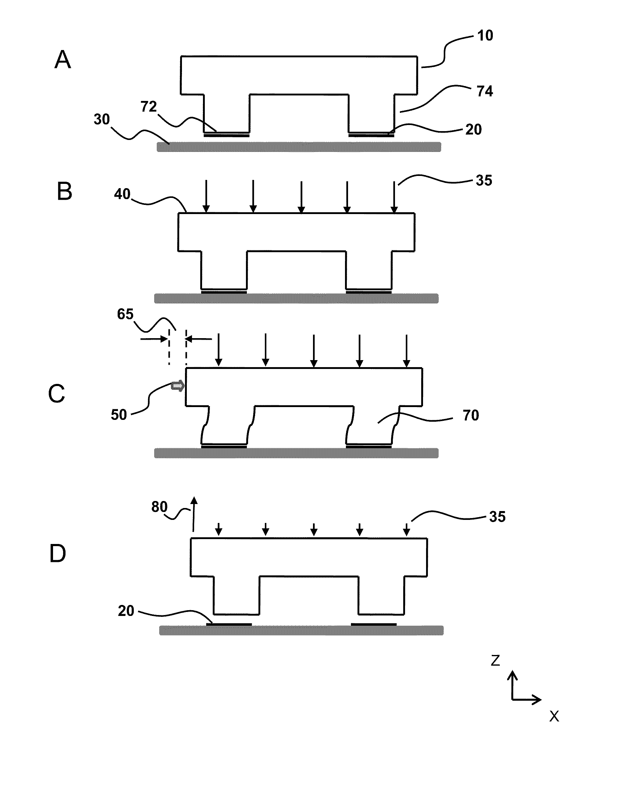
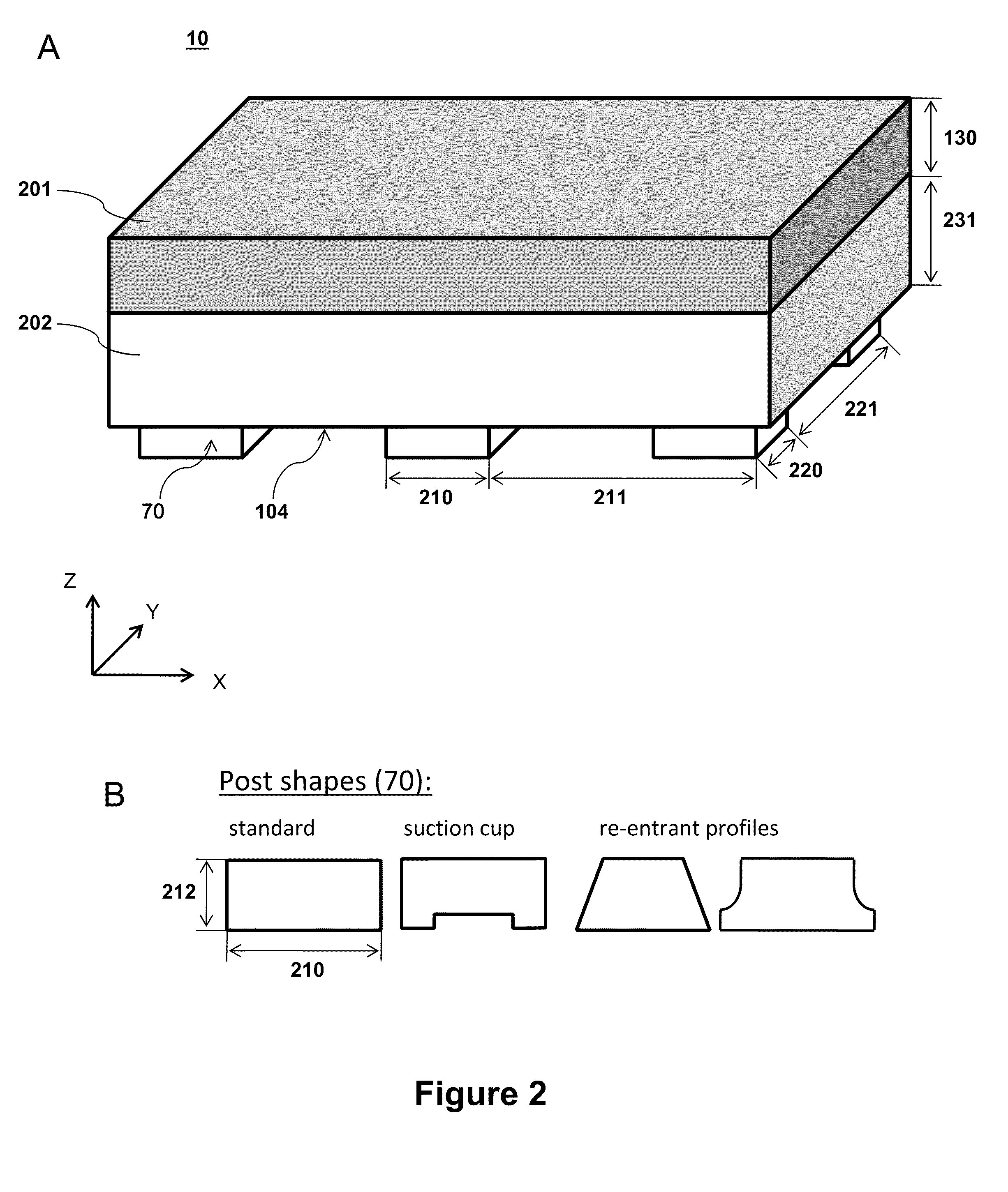
[0047]“Printing” refers to a process of transferring a feature, such as a semiconductor element, from a first surface to a second surface. In an aspect, the first surface is a donor surface and the second surface a receiving surface, and the transfer is mediated by an intermediate surface such as a stamp having a transfer surface. In an aspect, the first surface is a transfer surface on a stamp to which one or more semiconductor elements are supported, and the stamp is capable of releasing the elements to a receiving surface on a target substrate, thereby transferring the semiconductor element. In an aspect, the printing is dry transfer printing of printable semiconductors, wherein the adhesive force between a solid object and the stamp surface is rate-sensitive.

[0048]“Stamp” refers to a component for transfer, assembly and / or integration of structures and materials via printing, for example dry transfer contact printing. Composite stamps, such as composite stamps disclosed in U.S. ...


PUM

PropertyMeasurementUnit
plane displacementaaaaaaaaaa
pressureaaaaaaaaaa

Abstract

Provided are methods and devices for transfer printing of semiconductor elements to a receiving surface. In an aspect, the printing is by conformal contact between an elastomeric stamp inked with the semiconductor elements and a receiving surface, and during stamp removal, a shear offset is applied between the stamp and the receiving surface. The shear-offset printing process achieves high printing transfer yields with good placement accuracy. Process parameter selection during transfer printing, including time varying stamp-backing pressure application and vertical displacement, yields substantially constant delamination rates with attendant transfer printing improvement.

Description

[0001]This application claims the benefit of U.S. Provisional Patent Application No. 61 / 116,136 filed Nov. 19, 2008, which is specifically incorporated by reference to the extent not inconsistent herewith.STATEMENT REGARDING FEDERALLY SPONSORED RESEARCH OR DEVELOPMENT[0002]This invention was made, at least in part, with United States governmental support awarded by National Science Foundation Grant IIP-0712017. The United States Government has certain rights in this invention.BACKGROUND OF THE INVENTION[0003]Semiconductor chip or die automated assembly equipments typically rely on the use of vacuum operated placement heads often referred to as vacuum grippers or pick-and-place tools. In their simplest embodiment, these placement heads typically consist of an open ended cylinder having a drilled nozzle surface which seals to the die to accomplish physical attachment. Semiconductor chips or die which are ultra thin, fragile, or too small cannot be economically handled by conventional ...

Claims


Application Information

Patent Timeline
Patent Type & Authority Patents(United States)
IPC IPC(8): B29C59/00
CPCH01L21/6835H01L24/75H01L24/83H01L24/95H01L21/67092H01L2924/12041H01L2224/7598H01L2924/0132H01L2924/01322H01L2924/01075H01L2924/01033H01L2924/01023H01L2924/01006H01L2924/01005H01L2924/14H01L2924/10349H01L2924/10336H01L2924/10329H01L2924/01082H01L2924/01032H01L2924/01029H01L2221/68354H01L2224/75303H01L2224/75305H01L2224/75315H01L2224/83192H01L2224/838H01L2924/01011H01L2924/01013H01L2924/0102H01L2924/01014H01L2924/01015H01L2924/01049H01L2924/01031H01L2924/01051H01L2924/00H01L2924/15788H01L24/97H01L21/027
Inventor MENARD, ETIENNE
Owner X DISPLAY CO TECH LTD
Why Eureka
Try Eureka