Microstructure photomultiplier assembly

a photomultiplier and microstructure technology, applied in the field of microstructure photomultipliers, can solve the problems of increasing the number of electrons, increasing the cost of these devices, and relatively small pmts and mcps, so as to promote the promote the efficient production of secondary electrons, and promote the effect of efficient transfer and acceleration of electrons

Inactive Publication Date: 2013-08-13
BUBBLE TECH INDS
View PDF40 Cites 0 Cited by
  • Summary
  • Abstract
  • Description
  • Claims
  • Application Information

AI Technical Summary

Benefits of technology

[0010]The MPA comprises a photocathode (which converts light into electrons and which is located in front of or on the front surface of the assembly), followed by an electron-multiplying plate, or series of plates, each made from an insulating substrate which does not emit sufficient contaminants to poison the photocathode. Each plate is coated on the front and rear faces with a conductive layer. In addition, the front face of each plate is further coated with a layer of secondary electron-emissive material which, when struck by an incoming electron, can produce secondary electrons. Each plate is perforated with channels (with non-conducting walls) and the number and geometry of these channels is designed to promote the efficient transfer and acceleration of electrons through the channel, under an applied voltage differential across the plate(s). The number of plates placed in series is determined by the desired degree of electron multiplication. At the exit of the last plate, an anode is located to collect the electrons and generate an electrical signal that can be read by conventional electronics. The anode can be a simple anode or can be a position-sensitive anode. The spacing between the photocathode, the electron-multiplying plates, and the anode is selected to promote the efficient transfer and acceleration of electrons across the assembly, as well as to promote the efficient production of secondary electrons.
[0011]The photocathode, electron-multiplying plate(s), and anode are all contained within a vacuum enclosure, which helps to protect the photocathode from poisoning due to contaminants. The enclosure may also contain getters (i.e. reactive materials which remove trace contaminants from within the enclosure) in order to extend the life of the photocathode. The portion of the vacuum enclosure in front of the photocathode is transparent to the incoming light signal.

Problems solved by technology

The application of high voltage to PMTs and MCPs creates strong electric fields that accelerate and focus the photoelectrons from the photocathode to strike an adjacent surface, coated with a special material that produces high secondary electron emissions, resulting in an increase in the number of electrons.
Due to technical and cost issues associated with their manufacturing processes, PMTs and MCPs are relatively small.
The complexity of manufacturing translates into fairly high costs for these devices, currently from several hundred dollars to well over a thousand dollars each.
For certain applications, where large area detectors are required, the use of PMTs or MCPs can become prohibitively expensive.
Unfortunately, CsI is sensitive to only UV radiation and not to visible light around 450 nm such as produced by many common scintillators.
Attempts to develop gas PMTs for visible light have been met with limited success (M. Balcerzk, D. Mormann, A. Breskin, B. K. Singh, E. D. C. Freitas, R. Chechik, M. Klin and M. Rappaport, Trans. Nucl. Sci. 50 (2003) 847-854) because the reactivity of the K—Cs—Sb limits the stability of the photocathode to only a few months, despite care in avoiding contaminant poisons.

Method used


Image

  • Microstructure photomultiplier assembly
  • Microstructure photomultiplier assembly
  • Microstructure photomultiplier assembly

Examples


Embodiment Construction

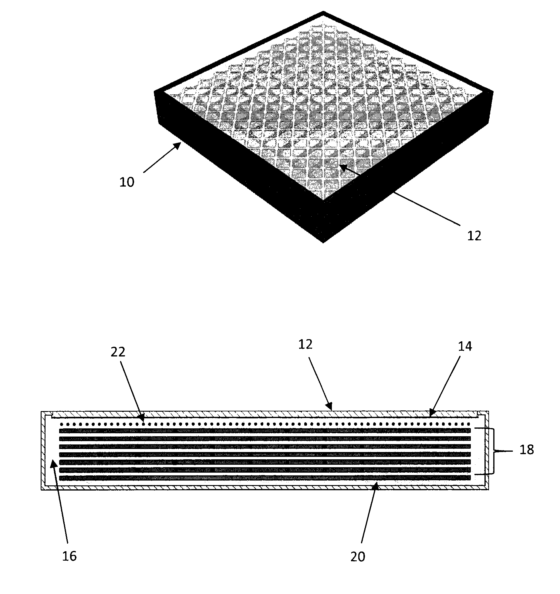
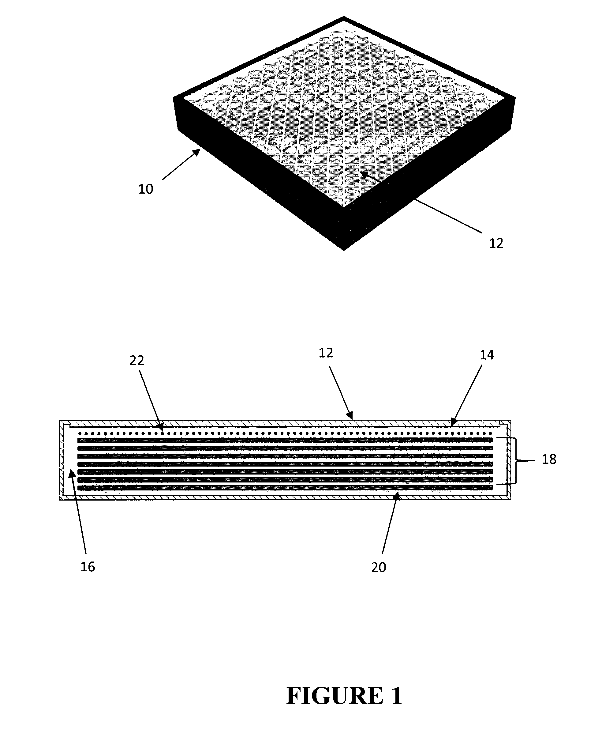
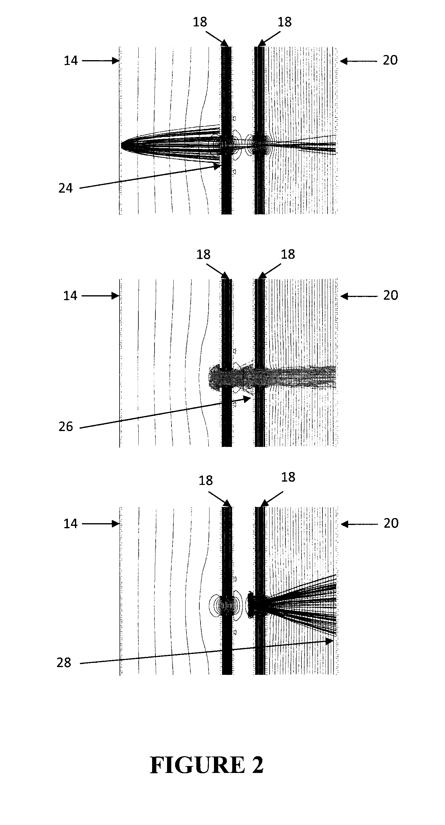
[0016]We propose to utilize circuit boards with small channels through them, similar to the basic component used by a GEM. However, we propose to deposit an additional layer of secondary electron emissive material on the conductive layer, among the holes, to form what is termed a multistructured board (MSB). This secondary emissive material can be a suitable alkali-based compound or a more robust compound that can be handled under non-vacuum conditions (e.g. see B. N. Laprade, R. Prunier and R. Farr, Poster paper 1340-17P, The Pittsburgh Conference 2005). This emissive material is only needed on one side of the board (the side facing the photocathode). The MPA is conceived to operate in a vacuum, like a conventional PMT. By applying a voltage across the board and maintaining a voltage between the photocathode and the front face of the MSB, photoelectrons from the photocathode will be drawn towards the board surface and be increased in energy by the electric field inside the channel....


PUM


Abstract

The Microstructure Photomultiplier Assembly (MPA) enables the effective conversion of light signals (received at the front of the assembly) into readily-detectable electrical signals. The MPA comprises a photocathode, followed by an electron-multiplying plate(s) made from an insulating substrate which does not emit sufficient contaminants to poison the photocathode. Each plate is coated with a conductive layer. The front face of each plate is further coated with a layer of secondary electron-emissive material which, when struck by an incoming electron, can produce secondary electrons. Each plate is perforated with channels. The channels are designed to promote the efficient transfer and acceleration of electrons through the channels, under an applied voltage differential across the plate(s). An anode (pixelated or non-pixelated) at the end of the last plate collects the electrons and generates an electrical signal. The MPA is contained within a vacuum enclosure.

Description

CROSS REFERENCE TO RELATED APPLICATIONS[0001]The present application claims priority to Canadian Patent Application No. 2,684,811 filed Nov. 6, 2009, which is incorporated by reference herein in its entirety.FIELD OF THE INVENTION[0002]The present invention, termed a Microstructure Photomultiplier Assembly (MPA) relates to the field of photo-detectors and in particular to devices commonly called photomultipliers or microchannel plates whose function is to convert a weak light signal, as may be emitted by certain radiation scintillators (e.g. a NaI(TI) crystal), to an electronic pulse that can be readily processed by conventional analogue and digital electronics. Such devices are also used in the detection of light signals associated with astronomy or optical communication.BACKGROUND OF THE INVENTION[0003]Detection of weak light signals is a common requirement in many areas of science and technology. The background that prompted the invention of the MPA is in the field of radiation d...

Claims


Application Information

Patent Timeline
Patent Type & Authority Patents(United States)
IPC IPC(8): H01J40/14H01J43/06
CPCH01J43/22
Inventor ANDREWS, HUGH ROBERTCLIFFORD, EDWARD T. H.FACINA, MARIUS EMANUELING, HARRYKOSLOWSKY, VERNON THEODORELOCKLIN, DARREN ADAMSMITH, MARTIN BERNARDSTEFANESCU, IRINA STEFANIA
Owner BUBBLE TECH INDS
Why Eureka
Try Eureka