Method and apparatus for controlling data transfer between EEPROM and a physical layer device

a technology of physical layer device and data transfer, which is applied in the field of data transfer, can solve the problems of difficult control of other devices that can share the bus, difficult to change pins and the configuration of physical layer devices, and long data transfer time, so as to facilitate efficient transfer of physical layer device configuration information, efficiently locate relevant data bytes, and reduce non-volatile memory access time

Active Publication Date: 2014-10-07
MARVELL INT LTD
View PDF23 Cites 0 Cited by
  • Summary
  • Abstract
  • Description
  • Claims
  • Application Information

AI Technical Summary

Benefits of technology

[0010]It is an object of the present invention to provide an IEEE 802.3 compliant physical layer device which facilitates efficient transfer of physical layer device configuration information with non-volatile memories in a physical layer device. According to the present invention, additional bits are provided in the volatile memory or memories in the physical layer device to indicate the status of data transfer. As a result, the system controller can read and write the non-volatile memories one byte at a time. When an error is detected, the system controller can efficiently locate the relevant data bytes without downloading the entire content of the non-volatile memories or uploading the entire content of the volatile memories. Consequently, the present invention reduces the non-volatile memory access time if a small number of data bytes in the non-volatile memory need to be accessed, and facilitates control of other devices sharing the bus with the non-volatile memory.
[0011]It is a further object of the present invention to provide an IEEE 802.3 compliant physical layer device which can be configured more flexibly. During reset time, the content of the non-volatile memories can be written to any PMA registers, PMD registers, PHY registers, and PCS (Physical Code Sublayer) registers. The present invention allows configuration of the physical layer devices flexibly after the physical layer device chip is made and reduces the number of chip pins used for configuration.
[0012]It is a further object of the present invention to provide an IEEE 802.3 compliant physical layer device which allows a system controller to directly access a non-volatile memory or a device sharing the bus with the non-volatile memory, bypassing a volatile memory in the physical layer device.
[0013]It is a further object of the present invention to provide an IEEE 802.3 compliant physical layer device which allows loading of configuration information of the physical layer device from a non-volatile memory to a volatile memory in the physical layer device without identifying the master.

Problems solved by technology

Consequently, the data transfer takes a long time and it is difficult to control other devices that can share the bus with an EEPROM.
After a chip is made, it is very difficult to change the pins and the configuration of the physical layer devices.

Method used


Image

  • Method and apparatus for controlling data transfer between EEPROM and a physical layer device
  • Method and apparatus for controlling data transfer between EEPROM and a physical layer device
  • Method and apparatus for controlling data transfer between EEPROM and a physical layer device

Examples


Embodiment Construction

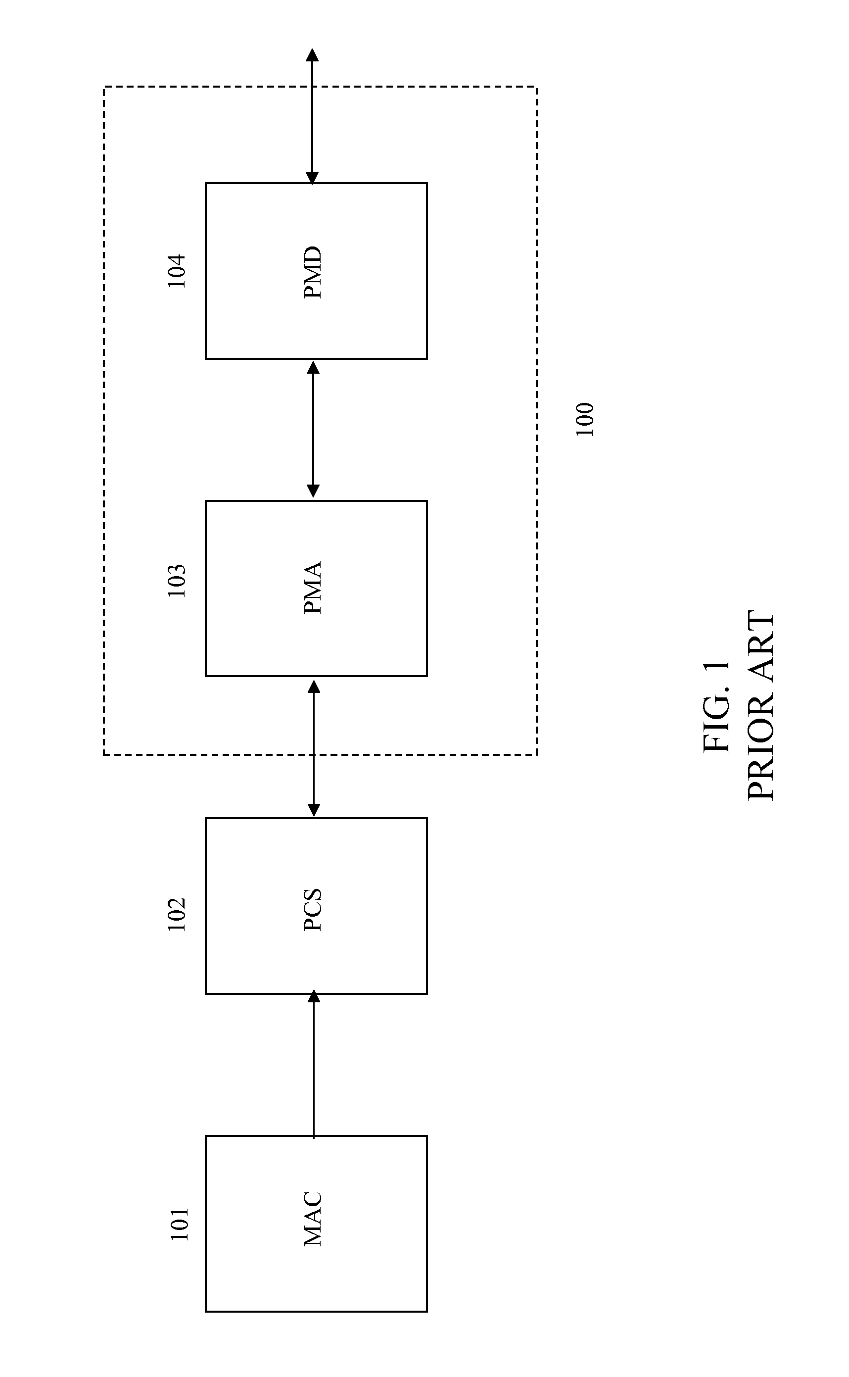
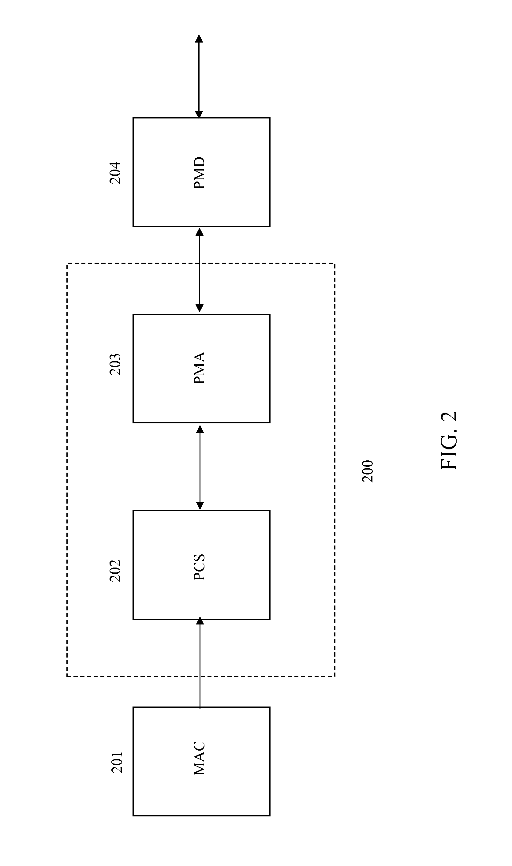
[0022]FIG. 2 shows a part of the 10 Gigabit Ethernet architecture employing one embodiment of the present application. The embodiment shown in FIG. 2 puts a PCS 202 and a PMA 203 into a chip 200. The chip 200 may be a CMOS chip. Thus, only half of the PMA PMD, a device according to the IEEE 802.3ae Standard, is outside the chip, while the other half is inside the chip. To enable the PCS 202 of the present invention to be IEEE 802.3ae Standard compliant, the chip 200 uses MDC (Management Data Clock) and MDIO (Management Data I / O) to communicate with a system controller, MAC (Media Access Control) sublayer 201, which controls the entire communication channel.

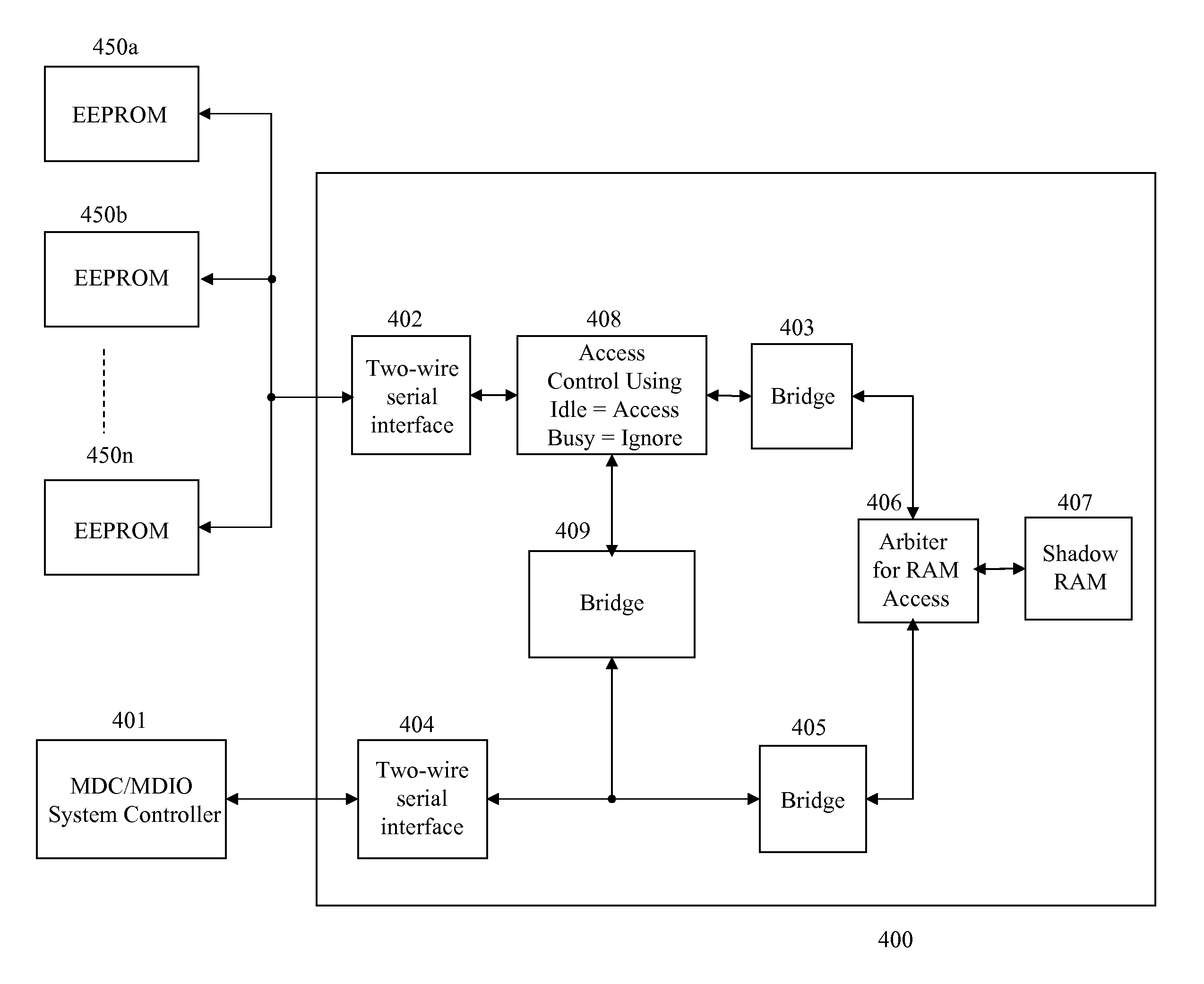
[0023]FIG. 3 shows a block diagram of an IEEE 802.3 compliant physical layer device according to one embodiment of the present invention. In one embodiment, a physical layer device 300 is configured according to the Xenpak Specification. Physical layer device configuration information and instructions used by a system controller 3...


PUM


Abstract

An IEEE 802.3 compliant physical layer device provides efficient loading of configuration information of the physical layer device. The configuration information is written into a volatile memory in the physical layer device, and then uploaded to at least one EEPROM. The configuration information is downloaded to the volatile memory during startup of the physical layer device. The system controller can also directly access the EEPROMs, bypassing the volatile memory. By providing a bridge between the system controller and the EEPROMs and providing additional bits in the volatile memory of the physical layer device, the system controller can read and write the EEPROMs one byte at a time. During reset time, the content of the EEPROMs is written to registers in the physical layer device to configure the physical layer device.

Description

CROSS-REFERENCE TO RELATED APPLICATIONS[0001]This application is a continuation of U.S. application Ser. No. 11 / 751,593 filed May 21, 2007, now U.S. Pat. No. 7,640,370, and which is a divisional of U.S. application Ser. No. 10 / 723,693 filed Nov. 25, 2003 (now abandoned).BACKGROUND OF THE INVENTION[0002]1. Field of the Invention[0003]The present invention relates to data transfer, and more specifically to efficiently controlling data transfer between non-volatile memories and an IEEE 802.3 compliant physical layer device.[0004]2. Description of the Related Art[0005]FIG. 1 shows a part of the 10 Gigabit Ethernet architecture according to the IEEE 802.3ae, Carrier Sense Multiple Access with Collision Detection (CSMA / CD) Access Method and Physical Layer Specification, 2002 (“the IEEE 802.3ae Standard”). A MAC (Media Attachment Control) sublayer 101 connects a chip 100 consisting of a PMA (Physical Media Attachment) sublayer 103 and a PMD (Physical Media Dependent) sublayer 104 through a...

Claims


Application Information

Patent Timeline
Patent Type & Authority Patents(United States)
IPC IPC(8): G06F13/00H04L12/66G06F13/36G06F13/14
CPCG06F13/1684
Inventor PHUNG, TRINH T.LO, WILLIAM
Owner MARVELL INT LTD
Why Eureka
Try Eureka