
Touch panel and method of detecting press operation position thereon
a technology of press operation and touch panel, which is applied in the field of touch panel, can solve the problems of complicated connection to electronic circuit and arithmetic processing for detecting position, long time for detecting position, etc., and achieve the effect of preventing the increase of the entire outer shape, and reducing the number of electrodes
- Summary
- Abstract
- Description
- Claims
- Application Information
AI Technical Summary
Benefits of technology
Problems solved by technology
Method used
Image

Examples
first exemplary embodiment
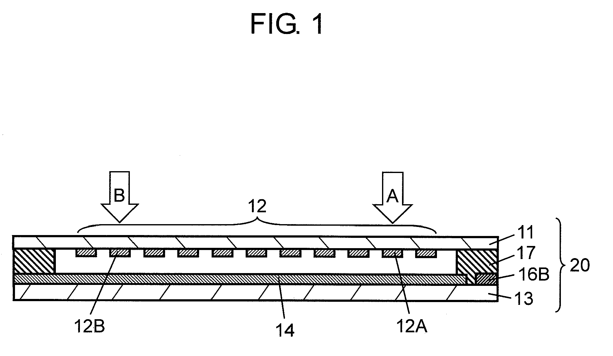
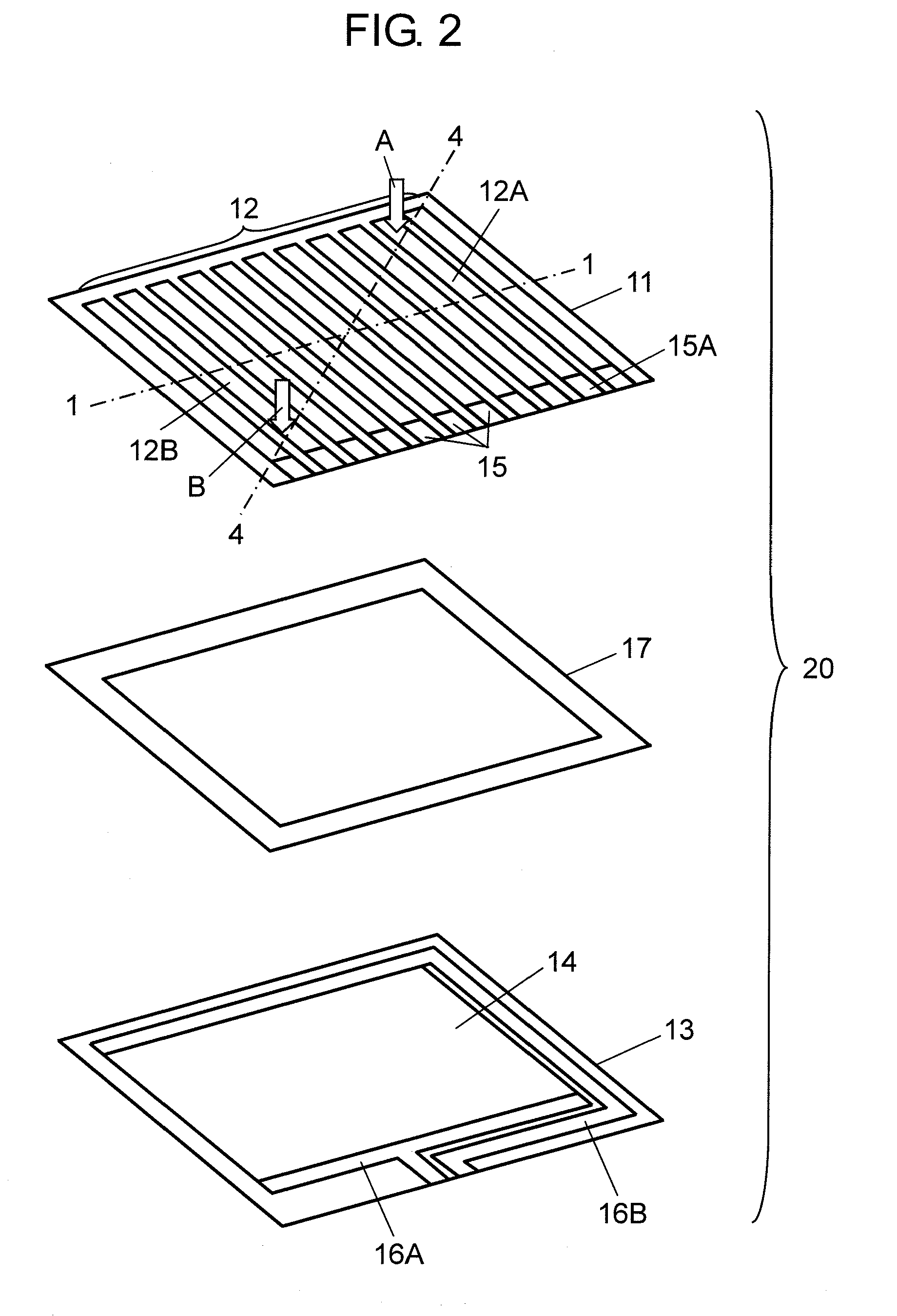
[0038]FIGS. 1 and 2 are a sectional view and an exploded perspective view of a touch panel in accordance with a first embodiment of the present invention. FIG. 1 shows a cross section taken on line 1-1 shown in FIG. 2. FIG. 3 is a diagram showing a connection between the touch panel and an electronic circuit. FIG. 4 is a conceptual view in a cross section taken on line 4-4 in FIG. 2. Touch panel 20 includes upper substrate 11, lower substrate 13 and spacer 17.
[0039]Light-transparent upper substrate 11 is made of light-transparent resin such as polyethylene terephthalate, polyether sulphone, and polycarbonate. Light transparent upper conductive layer 12 made of indium tin oxide, oxide tin, or the like, is formed on the bottom surface of upper substrate 11 by sputtering or the like. Upper conductive layer 12 is formed of belt-shaped conductive layers 12A, 12B and the other belt-shaped conductive layers, each formed in a width of about 0.3-2 mm with an interval of about 0.6-4 mm. On th...
second exemplary embodiment
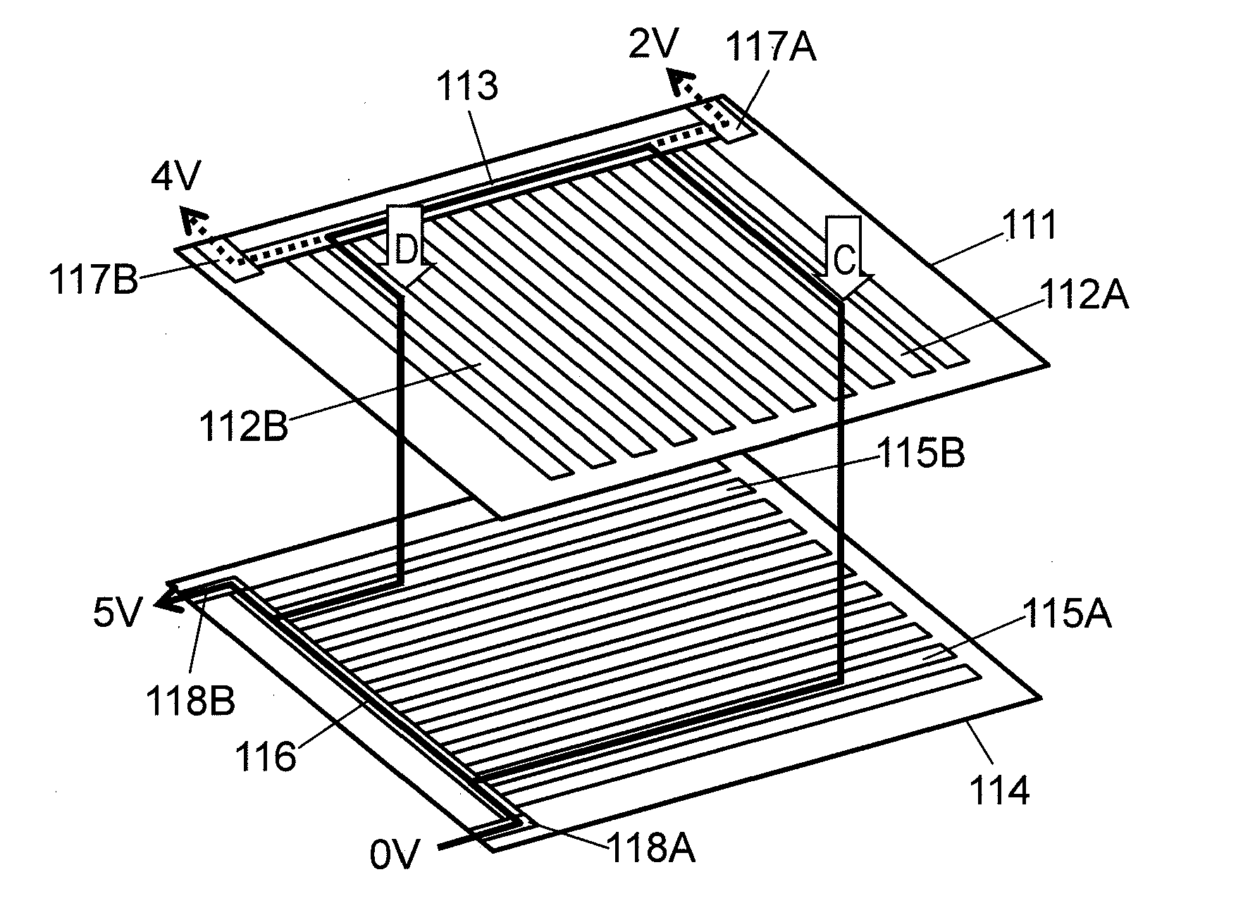
[0065]FIGS. 11 and 12 are a sectional view and an exploded perspective view showing a touch panel in accordance with a second embodiment of the present invention. FIG. 13 is a diagram showing a connection between the touch panel and an electronic circuit. Touch panel 130 includes upper substrate 111, a plurality of belt-shaped upper conductive layers 112, upper resistive layer 113, first upper electrode 117A, second upper electrode 117B, lower substrate 114, a plurality of belt-shaped lower conductive layers 115, lower resistive layer 116, first lower electrode 118A, second lower electrode 118B, and spacer 119.
[0066]Light-transparent upper substrate 111 is made of polyethylene terephthalate, polyether sulphone, or polycarbonate. Belt-shaped upper conductive layers 112 are formed on the bottom surface of upper substrate 111. Upper conductive layers 112 are made of indium tin oxide, oxide tin, or the like, and formed in the front-rear direction by sputtering or the like. Upper resisti...
PUM
 Abstract
Description
Claims
Application Information