Drop discharge apparatus, method for forming pattern and method for manufacturing semiconductor device

a technology of forming pattern and drop discharge, which is applied in the direction of vacuum evaporation coating, coating, printing, etc., can solve the problems of insufficient measures, display irregularities and display defects, and the accuracy of excessive drop landing is required beyond the need, so as to improve pattern accuracy, reduce production cost, and simplify manufacturing processes

Inactive Publication Date: 2013-09-10
SEMICON ENERGY LAB CO LTD
View PDF230 Cites 3 Cited by
  • Summary
  • Abstract
  • Description
  • Claims
  • Application Information

AI Technical Summary

Benefits of technology

[0006]Against the above-described problem, a performance of the drop discharge apparatus itself is improved significantly. That is, by semiconductor fine fabrication using a photolithography process and a focused ion beam, a high-precision drop discharge apparatus is manufactured, and fluctuation of sizes of discharged drops and fluctuation of discharge angles, due to the apparatus, are getting smaller.
[0032]Further, even comparing with a screen printing, development to a large size substrate is easy, and it is possible to lower product unit price, and it is possible to maintain high-resolution pattern formation, and to form a pattern with high utilization efficiency of materials.

Problems solved by technology

On the occasion of applying the above-described drop discharge method to pattern formation of a semiconductor field, excessive drop landing accuracy is required beyond that needed, for depiction of types and images.
In particular, in an image display device which is configured by TFT formed by an amorphous semiconductor film (amorphous silicon TFT) and TFT formed by a crystalline semiconductor film (polysilicon TFT), fluctuation of sizes of patterns and location accuracy of patterns influence great deal to an image display characteristic, and cause display irregularity and display defect.
On one hand, with regard to position control after drops, which were discharged from a drop discharge apparatus, landed on a substrate to be processed, sufficient measures have not found.
Inversely, when the landed drops is of liquid-attracting to the surface of the substrate to be processed, and the contact angle of the drops and the substrate is small, the drops after they were landed easily stretch out on the substrate, and it is difficult to control diameters of drops after they were landed, and fluctuation of drop diameters after they were solidified is large.

Method used


Image

  • Drop discharge apparatus, method for forming pattern and method for manufacturing semiconductor device
  • Drop discharge apparatus, method for forming pattern and method for manufacturing semiconductor device
  • Drop discharge apparatus, method for forming pattern and method for manufacturing semiconductor device

Examples


embodiment mode 1

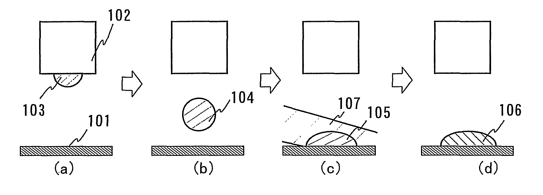
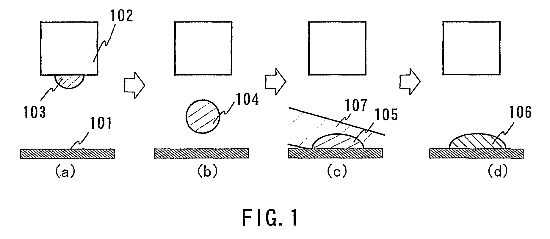
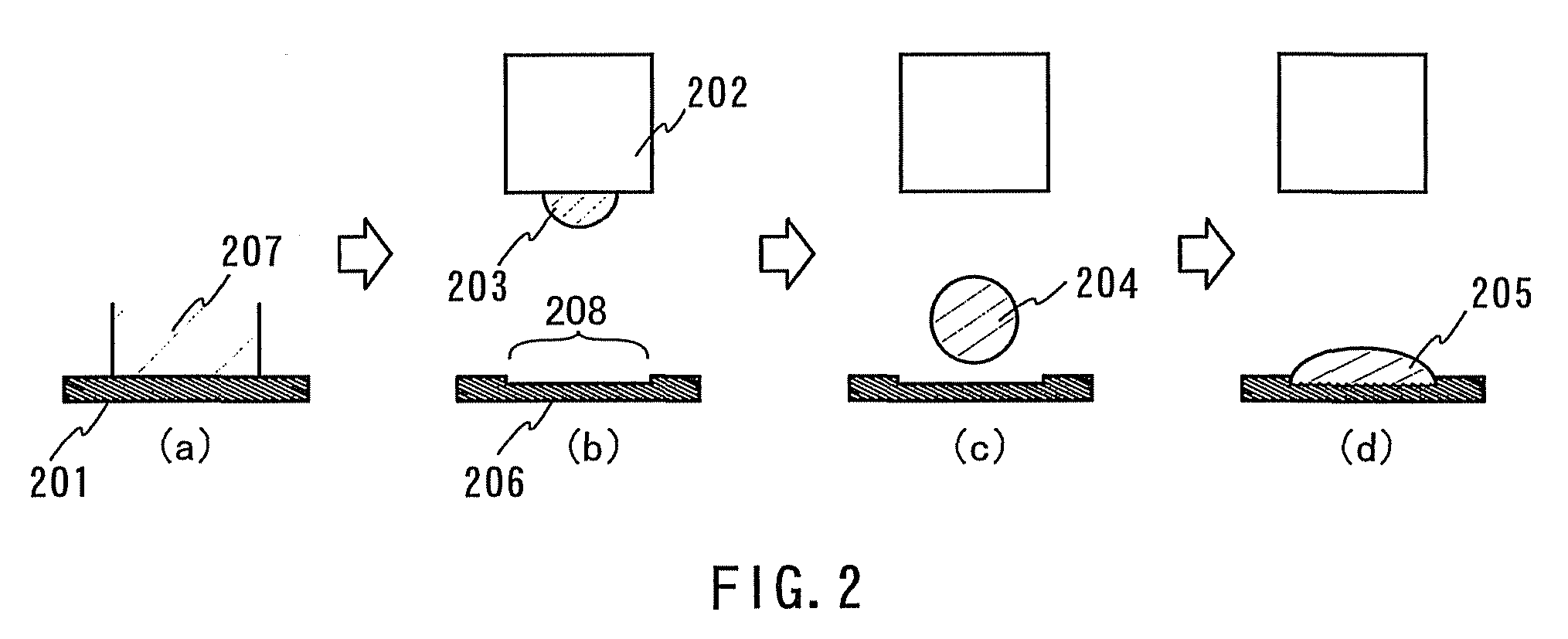
[0049]By use of FIGS. 1 to 4, a method for manufacturing a semiconductor device by use of a drop discharge apparatus in which pattern accuracy was heightened by carrying out irradiation of a laser beam will be explained. FIG. 1 typically shows a positional relationship in case that a substrate 101 to be processed and a front edge 102 of a drop discharge part and a drop 103 were viewed from the side. The drop discharge part is composed of a piezoelectric element (piezo element), a drop chamber, a discharge outlet (nozzle, head) and so on, and by applying a predetermined pulse voltage to the piezo element, the piezo element is deformed, to apply pressure to the drop chamber, and a drop is discharged from the discharge outlet.

[0050]As a drop to be discharged, used is a thing in which an electrically conductive material, which was properly selected from an element selected from tantalum (Ta), tungsten (W), titanium (Ti), molybdenum (Mo), aluminum (Al), copper (Cu), chromium (Cr), niobiu...

embodiment mode 2

[0060]One example of a drop discharge apparatus, which is used for carrying out the above-described embodiment mode, will be explained by use of FIG. 5 through FIG. 7.

[0061]A drop discharge apparatus, which is shown in FIG. 5, FIG. 6, has drop discharge means 501, 601 in the apparatus, and is such a thing that, by discharging solution by this, a desired pattern is formed on substrates 502, 602. Although it is not shown in the figure, in the drop discharge apparatus, a nozzle drive power supply and a nozzle heater for carrying out drop discharge are incorporated, and in addition, it is equipped with moving means for moving drop discharge means. In this drop discharge apparatus, as the substrate 502, 602, the substrates, which were described in the embodiment mode 1, can be applied.

[0062]In FIG. 5, FIG. 6, the substrates 502, 602 are carried from carry-in entrances 503, 603 in insides of housings 504, 604. The substrates 502, 602 are located on a transfer table which was equipped with...

embodiments

Embodiment 1

[0070]An embodiment 1 will be explained in detail by use of FIGS. 8 (A)˜(D). In this regard, however, this invention is not limited to the following explanation, and it is easily understood to persons with skill in the art to be able to change variously, without departing from a theme of this invention and a scope thereof, details thereof. Therefore, this invention is not a thing which is interrupted to be limited to a description content of embodiments which are shown below. Here, a manufacturing process for forming a drive TFT and a switch TFT and a capacitance on an identical substrate by use of this invention will be explained.

[0071]As a substrate 800, it is possible to use the substrates which were described in the embodiment mode 1. In this embodiment, a glass substrate (Corning Corporation make, #7059) is used. Subsequently, on the substrate 800, a base film 801, which is composed of an insulating film, is formed. The base film 801 may be any one of a single layer...


PUM

PropertyMeasurementUnit
diameteraaaaaaaaaa
pressureaaaaaaaaaa
diametersaaaaaaaaaa

Abstract

In this invention, it provides a method for forming a pattern, which is capable of improving position control after a drop, which was discharged from a drop discharge apparatus, was landed on a substrate. In addition, it provides a drop discharge apparatus which is capable of improving drop position accuracy after it was landed. Further, it provides a method for manufacturing a semiconductor device which uses the drop discharge apparatus of this invention.This invention is characterized in that a drop which was discharged from a discharge part, or a substrate on which a drop is landed, is irradiated with a laser beam, and a landing position of a drop is controlled. By this invention, it is possible to form a pattern, without using a photolithography process.

Description

[0001]This application is a divisional of application Ser. No. 10 / 827,710 filed on Apr. 20, 2004 now U.S. Pat. No. 7,585,783.TECHNICAL FIELD[0002]This invention relates to a drop discharge apparatus which is used for pattern formation of a semiconductor device. In addition, it relates to a method for forming a patter which is manufactured by use of the drop discharge apparatus according to this invention and a method for manufacturing a semiconductor device.BACKGROUND OF THE INVENTION[0003]A drop-on-demand type drop discharge technology, which is typified by a piezo type and a thermal jet type, or a continuous type drop discharge technology is gathering attention. This drop discharge technology has been used for depiction of types, images, but in these years, trials for applying this drop discharge technology to a semiconductor field such as fine pattern formation, a bio, medical field such as DNA chip fabrication, a chemical, medical field such as micro-chemical chip fabrication ha...

Claims


Application Information

Patent Timeline
Patent Type & Authority Patents(United States)
IPC IPC(8): B05B5/00B05B3/00B05B9/06B05C5/00C23C14/00H01L21/288H01L21/336H01L21/768H01L21/77H01L21/84H01L27/12
CPCH01L21/288H01L21/76838H01L21/76877H01L27/1292H01L29/66757H01L29/66765H01L27/1285H01L27/12B41J2/17B82Y99/00
Inventor NAKAMURA, OSAMUYAMAZAKI, SHUNPEI
Owner SEMICON ENERGY LAB CO LTD
Why Eureka
Try Eureka