
Gate signal line driving circuit and display device with suppression of changes in the threshold voltage of the switching elements

a signal line driving circuit and switching element technology, applied in the direction of digital storage, instruments, computing, etc., can solve the problems of deteriorating display performance, low voltage application switching element swa not being sufficiently turned on in response to signal low period, unstable potentials of nodes nb>1/b> and nb>2/b> at the startup of the display device, etc., to achieve the effect of suppressing deterioration of display performan

Active Publication Date: 2013-09-24
PANASONIC INTELLECTUAL PROPERTY CORP OF AMERICA +1
View PDF5 Cites 4 Cited by
  • Summary
  • Abstract
  • Description
  • Claims
  • Application Information

AI Technical Summary

Benefits of technology

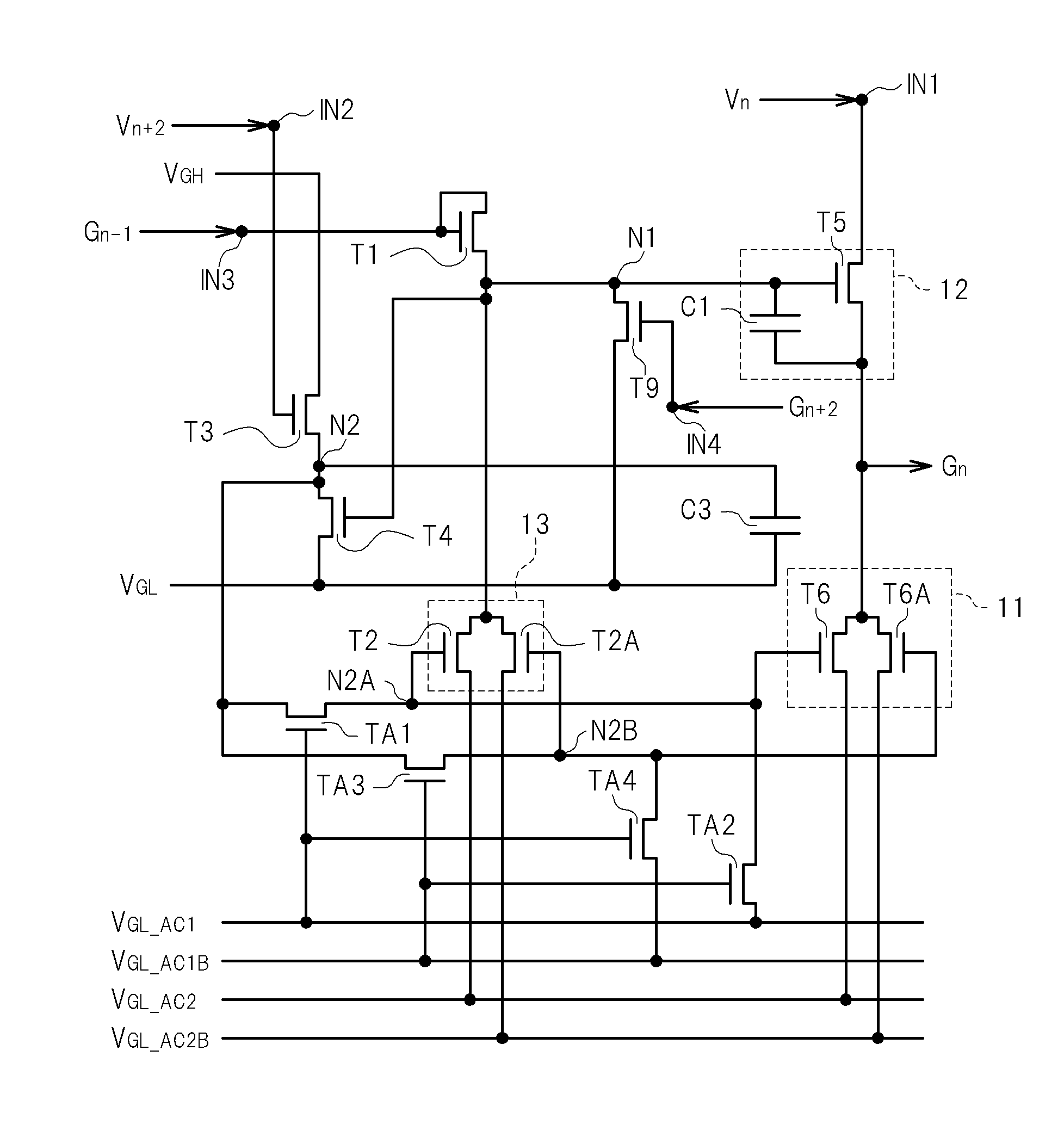
[0022]The invention has been made in view of the problems, and aims to provide a gate signal line driving circuit capable of suppressing deterioration of performance caused by the Vth shift in the startup reset transistor and other transistors that constitute a shift register circuit and a display device using the same.
[0033]According to the invention, a gate signal line driving circuit capable of suppressing deterioration of display performance caused by the Vth shift in the startup reset transistor and other transistors that constitute a shift register circuit and a display device using the same are provided.

Problems solved by technology

Moreover, the potentials of the nodes N1 and N2 are unstable at the startup of the display device.
Thus, off-leakage, malfunctioning, and the like are likely to occur, which may cause deterioration of a display performance.
Moreover, for example, when the Vth shift occurs in the low voltage application switching element SWA and the like and the threshold voltage Vth thereof exceeds a critical value, the low voltage application switching element SWA is not sufficiently turned ON in response to the signal low period.
When noise is superimposed on the gate signal, even during the signal low period, a display data voltage which should be written to other pixels is written to pixels connected to the gate signal line, and a display performance deteriorates.

Method used


Image

  • Gate signal line driving circuit and display device with suppression of changes in the threshold voltage of the switching elements
  • Gate signal line driving circuit and display device with suppression of changes in the threshold voltage of the switching elements
  • Gate signal line driving circuit and display device with suppression of changes in the threshold voltage of the switching elements

Examples


Embodiment Construction

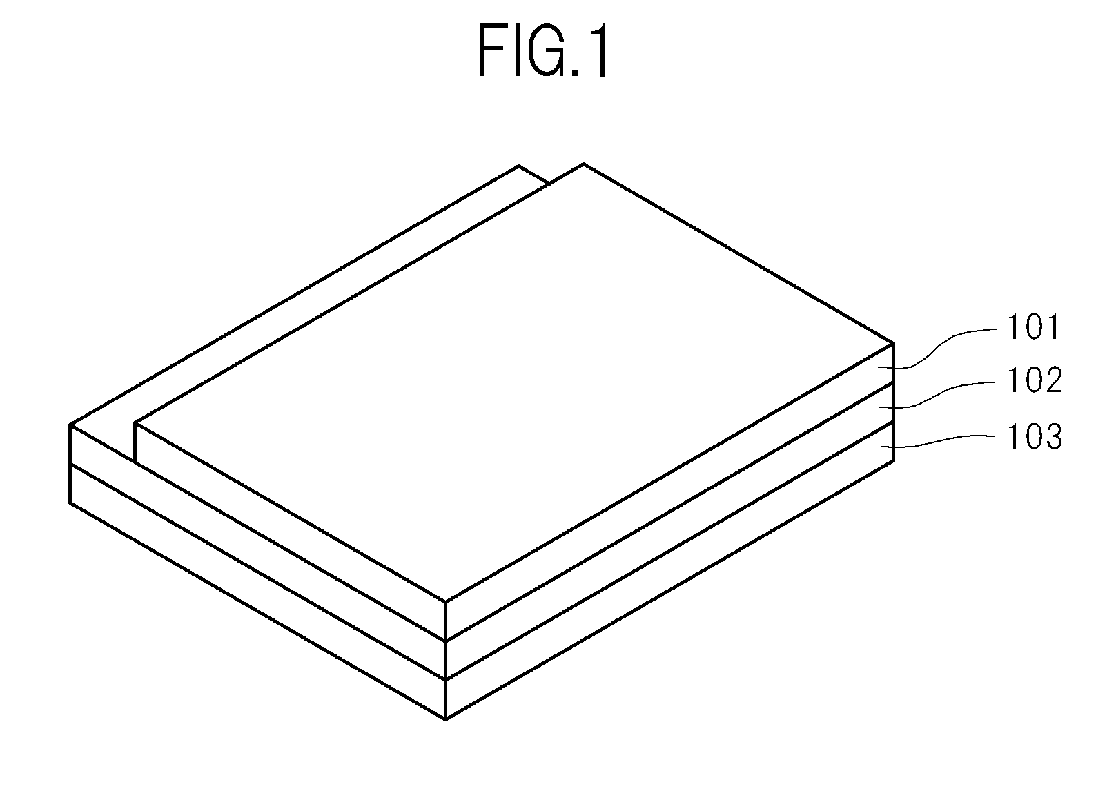
[0049]A display device according to an embodiment of the invention is an IPS (In-Plane Switching)-mode liquid crystal display device. FIG. 1 is a general perspective view of a liquid crystal display device according to the embodiment of the invention. The liquid crystal display device shown in FIG. 1 includes a TFT substrate 102, on which gate signal lines 105, video signal lines 107, pixel electrodes 110, common electrodes 111, TFTs 109, and the like, described later, are disposed; a filter substrate 101 which faces the TFT substrate 102 and in which color filters are provided; a liquid crystal material sealed in a region which is interposed by the two substrates; and a backlight 103 which is positioned in contact with a side of the TFT substrate 102 opposite the filter substrate 101.

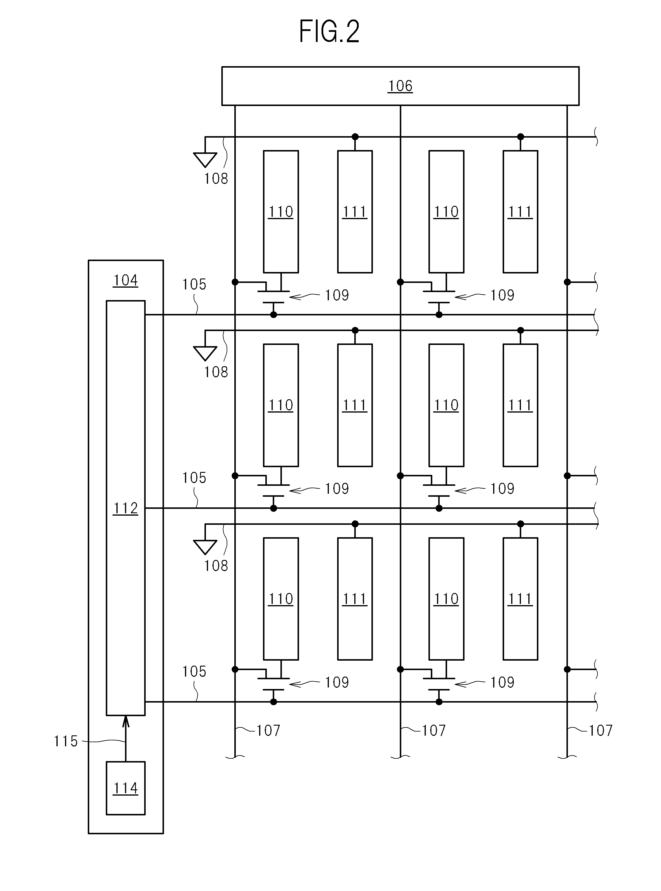
[0050]FIG. 2 is a schematic diagram showing an example of an equivalent circuit of the TFT substrate 102. In FIG. 2, on the TFT substrate 102, a number of gate signal lines 105 connected to a gate sign...


PUM


Abstract

A gate signal line driving circuit and a display device includes first and second low voltage application switching elements that supply a low voltage to gate signal lines, a holding capacitor that is connected to a reset target node and supplies an ON signal towards the first and second low voltage application switching elements in a signal low period, first and third control switching elements the one ends of which are connected to the switch input of the first or second low voltage application switching element, and second and fourth control switching elements which each are provided between the switch input of the first or second low voltage application switching element and one end of the holding capacitor. In a startup period, a high voltage is supplied to the holding capacitor through the first to fourth control switching elements.

Description

CROSS-REFERENCE TO RELATED APPLICATION[0001]The present application claims priority from Japanese application JP2009-295516 filed on Dec. 25, 2009, the content of which is hereby incorporated by reference into this application.BACKGROUND OF THE INVENTION[0002]1. Field of the Invention[0003]The present invention relates to a gate signal line driving circuit and a display device using the same. More particularly, the invention relates to suppression of changes in the threshold voltage of the switching elements of a gate signal line driving circuit and improvement in the display performance of a display device using the switching elements.[0004]2. Description of the Related Art[0005]In display devices such as liquid crystal display devices, there are cases where a display device with an internal shift register has been adopted. The display device with an internal shift register has a configuration in which shift register circuits provided in a gate signal line driving circuit that scan...

Claims


Application Information

Patent Timeline
Patent Type & Authority Patents(United States)
IPC IPC(8): G09G3/36
CPCG09G3/3677G11C19/184G09G2300/0426
Inventor SHIBATA, TAKESHIKOTANI, YOSHIHIROOCHIAI, TAKAHIROGOTO, MITSURU
Owner PANASONIC INTELLECTUAL PROPERTY CORP OF AMERICA
Learn More