Semiconductor device and driving circuit

a driving circuit and semiconductor technology, applied in the direction of transistors, pulse generators, pulse techniques, etc., can solve the problems of large fluctuation of the potential of the ac output terminal out, loss due to the current passing through the high breakdown voltage mosfet, and reduce the breakdown voltage. , to achieve the effect of reducing the displacement current, and reducing the output capacitan

Active Publication Date: 2013-10-01
FUJI ELECTRIC CO LTD
View PDF27 Cites 1 Cited by
  • Summary
  • Abstract
  • Description
  • Claims
  • Application Information

AI Technical Summary

Benefits of technology

[0073]In order to solve the foregoing problems with the related-art technologies, it is an object of this invention to provide a semiconductor device with a high switching response speed. Further, in order to solve the foregoing problems with the related-art technologies, it is another object of this invention to provide a driving circuit suppressed in power loss and malfunction.
[0098]By using such a structure, in order for the high breakdown voltage MOSFET to ensure the high breakdown voltage, for example, when the breakdown voltage region forming a circular planar shape has an area equivalent to or larger than that for the current driving ability required of the MOSFET, the parasitic capacitance component in the breakdown voltage region except for the necessary current ability and the like can be nullified according to the switching frequency of the actual use conditions. This can reduce the output capacitance of the high breakdown voltage MOSFET inexpensively. For this reason, when for a level shift circuit, a high breakdown voltage MOSFET is used, it is possible to reduce the displacement current upon the occurrence of a dV / dt surge.
[0099]Further, in accordance with the foregoing invention, by reducing the output capacitance of the high breakdown voltage MOSFET, it is possible to accelerate the discharge of the output capacitance upon inputting of an ON signal to the gate of the high breakdown voltage MOSFET. Still further, when the high breakdown voltage MOSFET is used for a level shift circuit, it is possible to shorten the turn on / turn off transfer delay time of the high-side driving circuit part. By shortening the transfer delay time, it also becomes possible to set small the on duty for driving the high breakdown voltage MOSFET.
[0100]Still further, in accordance with the foregoing invention, it is possible to set small the on duty for driving the high breakdown voltage MOSFET. Therefore, it is possible to reduce the load resistance portion for level shift of the high breakdown voltage IC while keeping the allowance loss of the package for resin sealing the high breakdown voltage IC. As a result, both of the current value of the displacement current upon the occurrence of the dV / dt surge and the resistance value of the load resistance portion become small while the power loss at the level shift circuit of the high breakdown voltage IC being suppressed. This results in the reduction of the voltage drop at the load resistance portion, which enables the implementation of a driving circuit less likely to malfunction due to the dV / dt surge.
[0101]The semiconductor device and the driving circuit in accordance with this invention exert an effect of capable of providing a semiconductor device with a high switching response speed. Further, the semiconductor device and the driving circuit in accordance with the present invention exert an effect of capable of providing a driving circuit suppressed in power loss and malfunction.

Problems solved by technology

However, particularly when the reference potential of the high potential side low breakdown voltage circuit portion fluctuating in reference potential as the circuit portion surrounded by the broken line of FIG. 16 is at a high potential, the loss due to the current passed through the high breakdown voltage MOSFETs 1 and 2 increases.
This results in a large fluctuation of the potential of the AC output terminal OUT.
However, there is the following problem.
Also with the high breakdown voltage MOSFET 11b, there occurs the same problem that the reduction of the PN junction area results in the reduction of the breakdown voltage as that with the high breakdown voltage MOSFET 11.

Method used


Image

  • Semiconductor device and driving circuit
  • Semiconductor device and driving circuit
  • Semiconductor device and driving circuit

Examples


embodiment 1

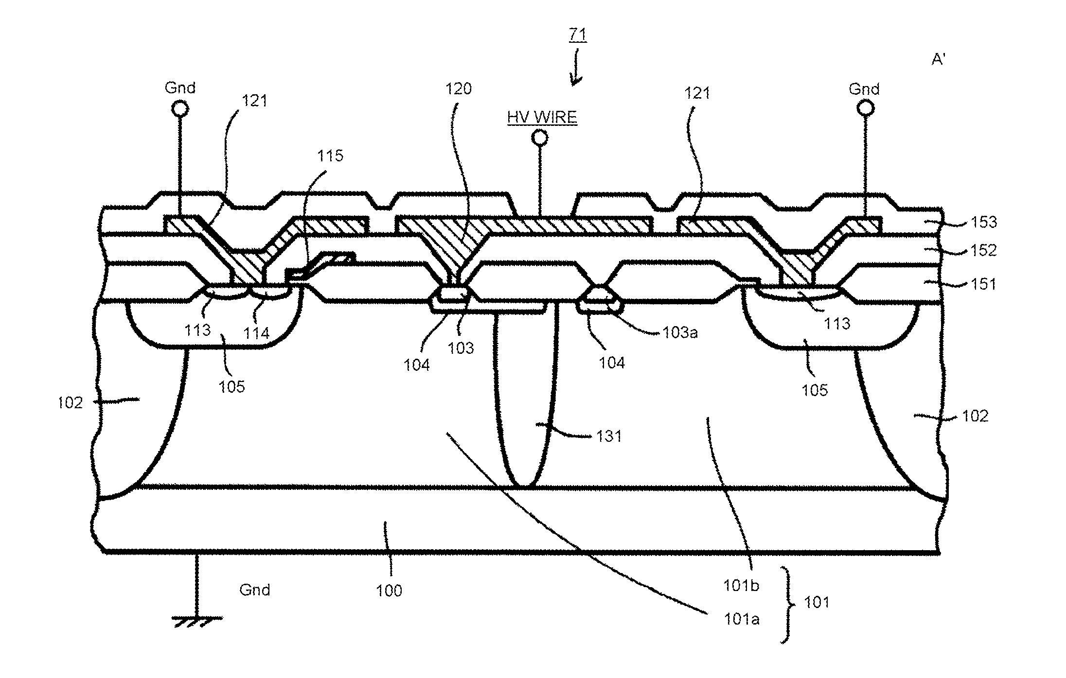
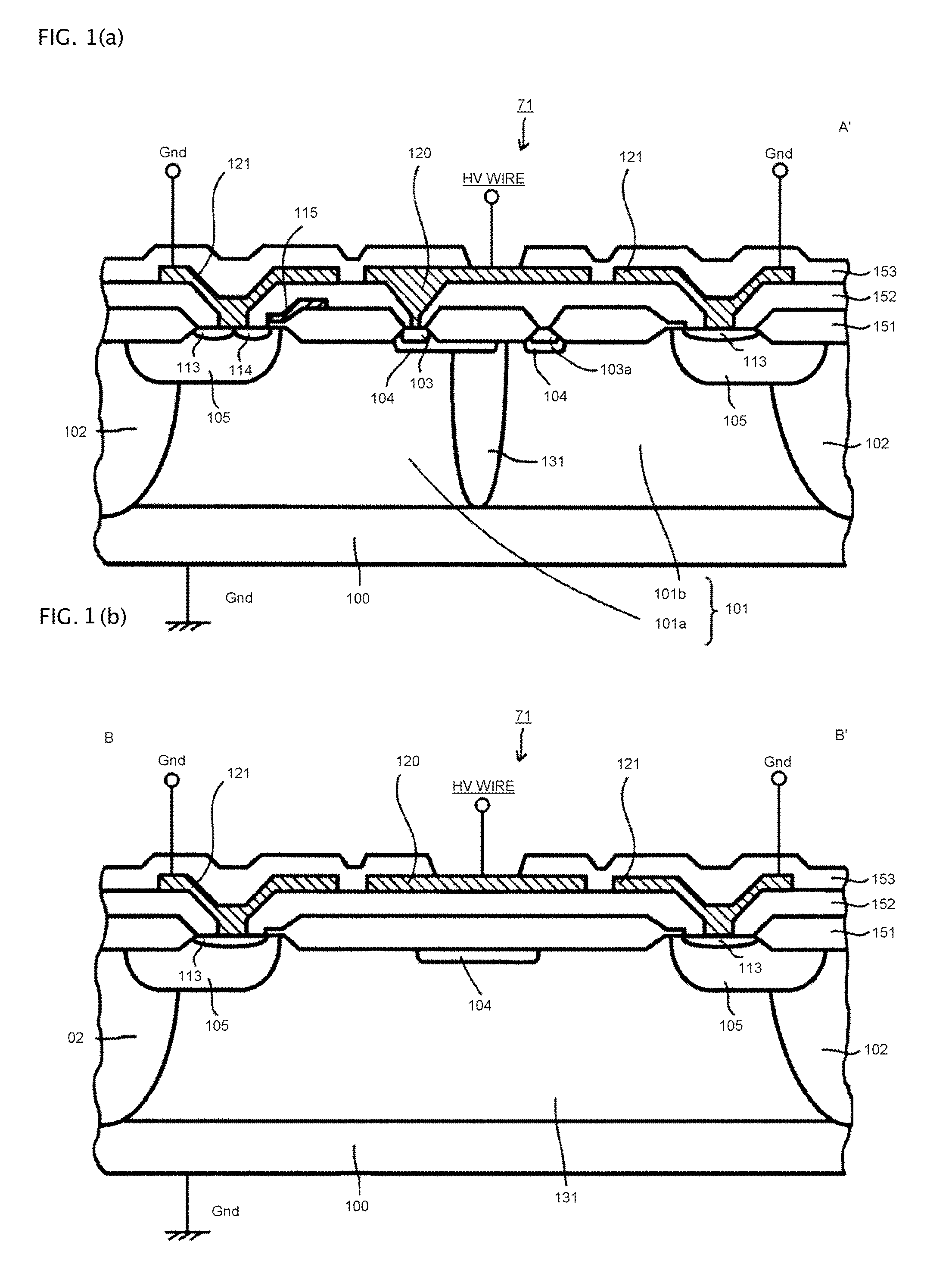
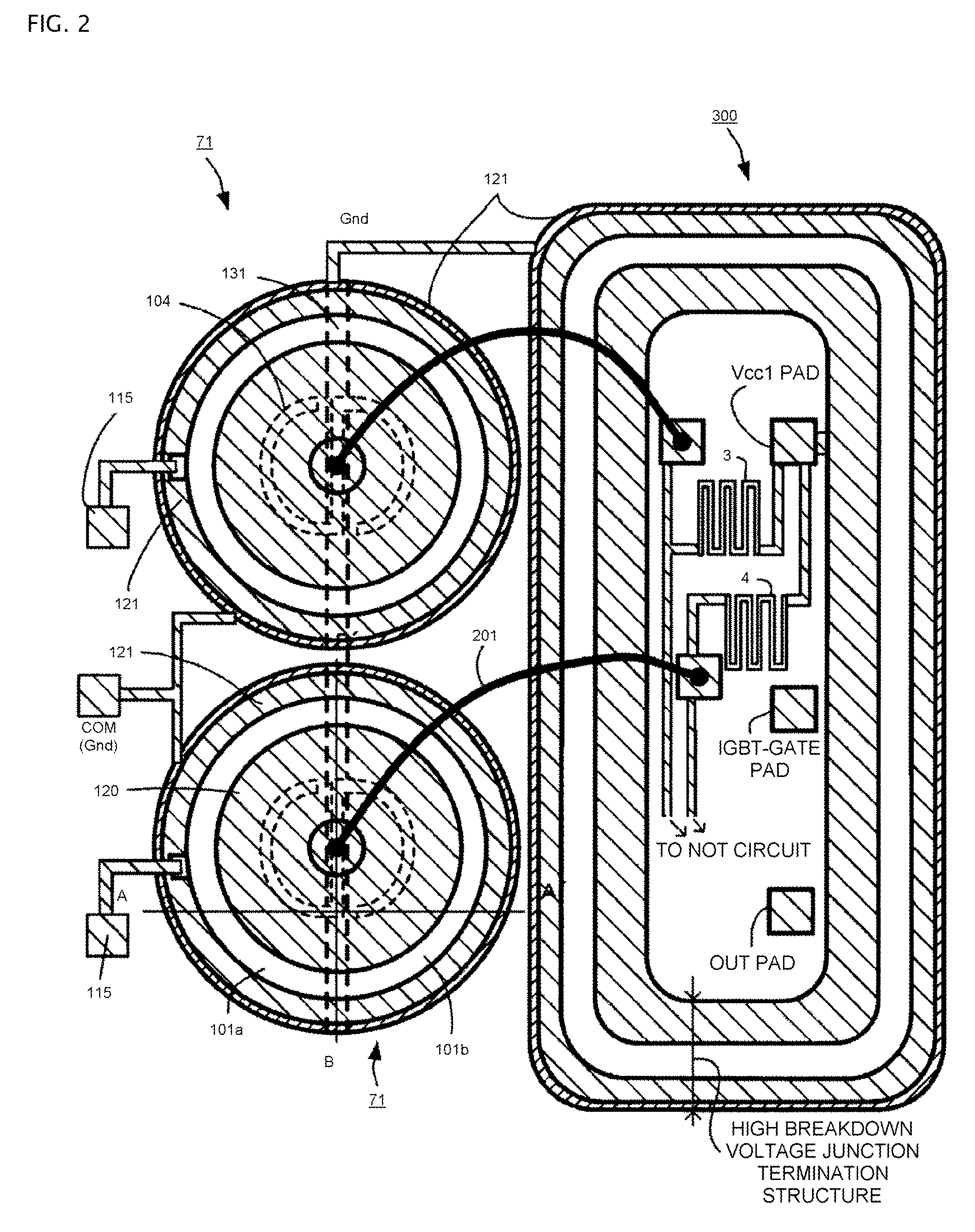
[0123]Referring to FIGS. 1 to 3 and FIG. 16, Embodiment 1 will be described. FIG. 1 is a cross-sectional view showing an essential part of a high breakdown voltage MOSFET in accordance with Embodiment 1 of the present invention. Whereas, FIG. 2 is a plan view showing an essential part of a high breakdown voltage IC in which a level shift circuit including high breakdown voltage MOSFETs in accordance with the present invention and a driving circuit including a floating potential region are formed in the same semiconductor substrate. The cross-sectional structure along the cut line A-A′ of FIG. 2 corresponds to the cross-sectional view shown in FIG. 1(a). The cross-sectional structure along the cut line B-B′ of FIG. 2 corresponds to the cross-sectional view shown in FIG. 1(b).

[0124]Whereas, FIG. 3 is a plan view showing a planar layout in the essential part of the high breakdown voltage MOSFET shown in FIG. 2. FIG. 3 shows only the planar layout of the region exposed at the surface of...

embodiment 2

[0170]Referring to FIGS. 6 and 7, a description will be given to a high breakdown voltage MOSFET in accordance with Embodiment 2. FIG. 6 is a cross-sectional view showing an essential part of the high breakdown voltage MOSFET in accordance with Embodiment 2 of the present invention. FIG. 7 is a plan view showing a planar layout in the essential part of the high breakdown voltage MOSFET shown in FIG. 6. FIG. 7 shows only the planar layout of the region exposed at the surface of the n− type region 101 of respective regions forming a high breakdown voltage MOSFET 72. The high breakdown voltage MOSFET 72 of FIG. 6 corresponds to the high breakdown voltage MOSFET 1 or 2 of FIG. 16.

[0171]The high breakdown voltage MOSFET 72 has the following respective regions. In the surface layer of the p−type silicon substrate 100, selectively, the n− type region 101 is formed. The n− type region 101 is formed by impurity diffusion. The surface concentration of phosphorus impurities of the n− type regi...

embodiment 3

[0205]FIG. 8 is a plan view showing an essential part of a high breakdown voltage IC in which a level shift circuit including high breakdown voltage MOSFETs in accordance with Embodiment 3 of the present invention and a driving circuit including a floating potential region are formed in the same semiconductor substrate. The cross-sectional structure along the cut line A-A′ of FIG. 8 is equal to the cross-sectional structure of the high breakdown voltage MOSFET shown in FIG. 1(a) of Embodiment 1. Incidentally, in FIG. 8, only the n offset region 104 and the p− region 131 of the semiconductor regions forming a high breakdown voltage MOSFET 73 are indicated with broken lines.

[0206]The high breakdown voltage MOSFET 73 of FIG. 8 is different from the high breakdown voltage MOSFET 71 of FIG. 2 in that the planar shape of the p−region 131 is formed in the V shape. The n type region 101 is divided into, for example, an n− type region 101a forming a fan-shaped planar shape formed of a minor ...


PUM


Abstract

A high breakdown voltage semiconductor device includes: an n− type region (101) surrounded by a p− well region (102) on a p− type silicon substrate (100); a drain n+ region (103) connected to a drain electrode (120); a p base region (105) formed so as to surround the drain n+ region (103); a source n+ region (114) formed in the p base region (105); and a p− region (131) for isolating the n− type region (101) into an n− type region (101a) including the drain n+ region (103), and an n− type region (101b) not having the drain n+ region (103). The n− type region (101b) is connected to the drain electrode (120) or the drain n+ region (103) via an n offset region (104) or a polysilicon (304) which is a high resistance element.

Description

[0001]This application is a U.S. National Phase Application of PCT International Application PCT / JP2011 / 061912 filed on May 24, 2011 which is based on and claims priority from JP2010-128499 filed on Jun. 4, 2010 the contents of which is incorporated herein in its entirety by reference.TECHNICAL FIELD[0002]The present invention relates to a semiconductor device and a driving circuit.BACKGROUND ART[0003]Power devices have been widely used in a large number of fields such as inverters for motor control, and furthermore, power source applications for large capacity PDPs (plasma display panels), liquid crystal panels, and the like, and inverters for home electrical appliances including air conditioners and light fixtures. Conventionally, driving and control of such power devices have been performed by an electronic circuit formed of a combination of semiconductor elements such as photo couplers and electronic components such as transformers.[0004]However, a recent advancement of a LSI (l...

Claims


Application Information

Patent Timeline
Patent Type & Authority Patents(United States)
IPC IPC(8): H01L27/088
CPCH01L27/0629H01L27/088H01L29/0878H01L29/7817H01L27/0823H01L29/0696H01L29/402H01L29/42368H01L2224/4813H01L2924/1305H01L2924/13055H01L2924/13091H01L2924/12032H01L2224/05554H01L2924/00
Inventor YAMAJI, MASAHARU
Owner FUJI ELECTRIC CO LTD
Why Eureka
Try Eureka