Optical semiconductor relay device

Inactive Publication Date: 2009-05-07
RENESAS ELECTRONICS CORP
View PDF3 Cites 5 Cited by
  • Summary
  • Abstract
  • Description
  • Claims
  • Application Information

AI Technical Summary

Problems solved by technology

This variance in time causes the transient voltages between the output terminals and these voltages may become the source of noise in other equipm

Method used


Image

  • Optical semiconductor relay device
  • Optical semiconductor relay device
  • Optical semiconductor relay device

Examples


example 1

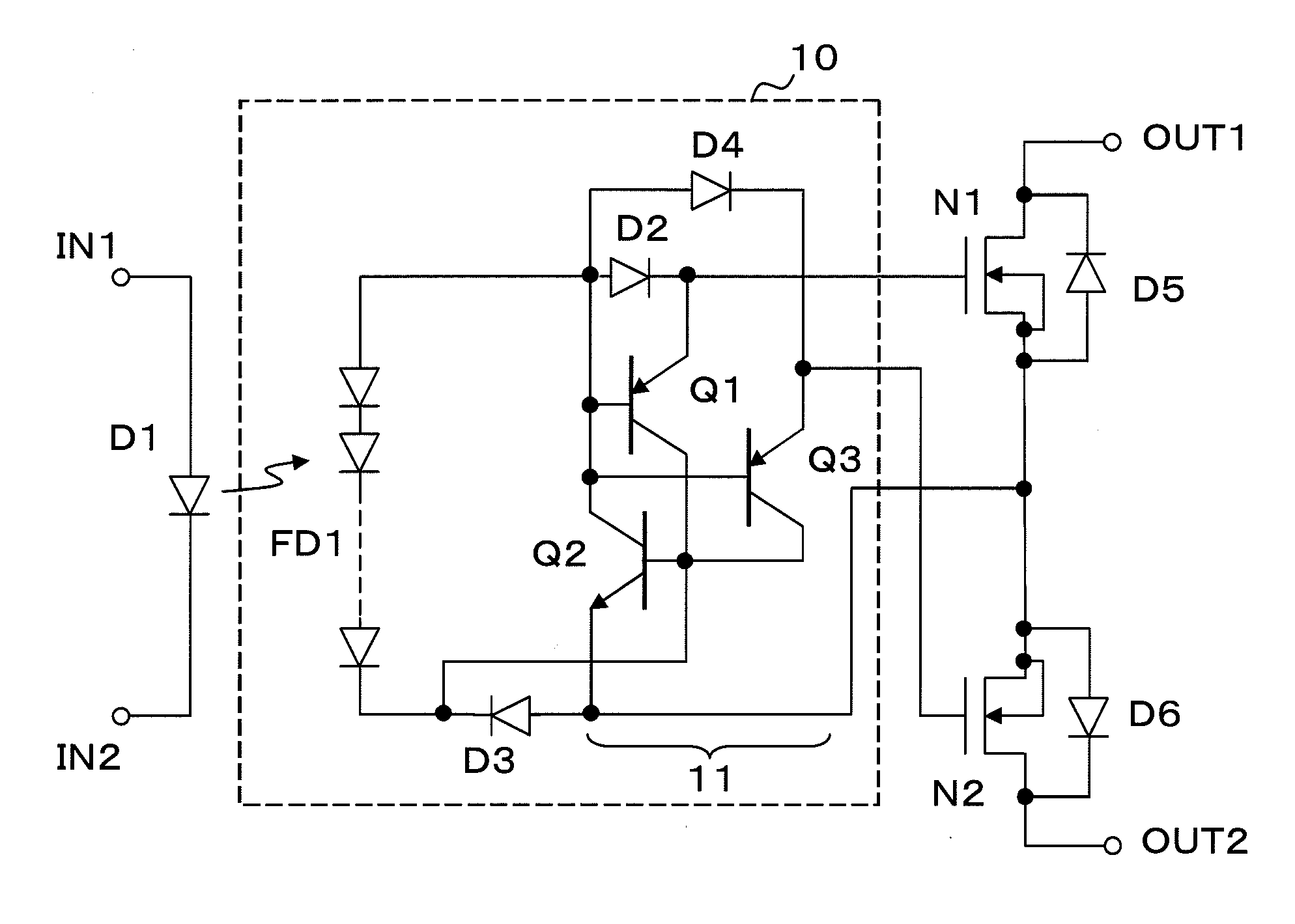
[0044]FIG. 1 is a circuit diagram of an optical semiconductor relay device relating to a first example of the present invention. In FIG. 1, the optical semiconductor relay device comprises a pair of input terminals IN1 and IN2, a pair of output terminals OUT1 and OUT2, MOSFETs N1 and N2 connected between the output terminals, and a drive circuit 10 connected between the input terminals IN1 and IN2 and the MOSFETs N1 and N2. An LED D1 is connected between the input terminals IN1 and IN2. Source electrodes of the MOSFETs N1 and N2 are electrically connected to each other, and drains are connected to the output terminals OUT1 and OUT2, respectively. Further, diodes D5 and D6 denote parasitic diodes of the MOSFETs N1 and N2 respectively.

[0045]The drive circuit 10 is configured so that gate electrodes of the MOSFETs N1 and N2 are not short-circuited to each other and a single control signal turns on / off the MOSFETs N1 and N2. Further, the drive circuit 10 includes a photodiode array FD1 ...

example 2

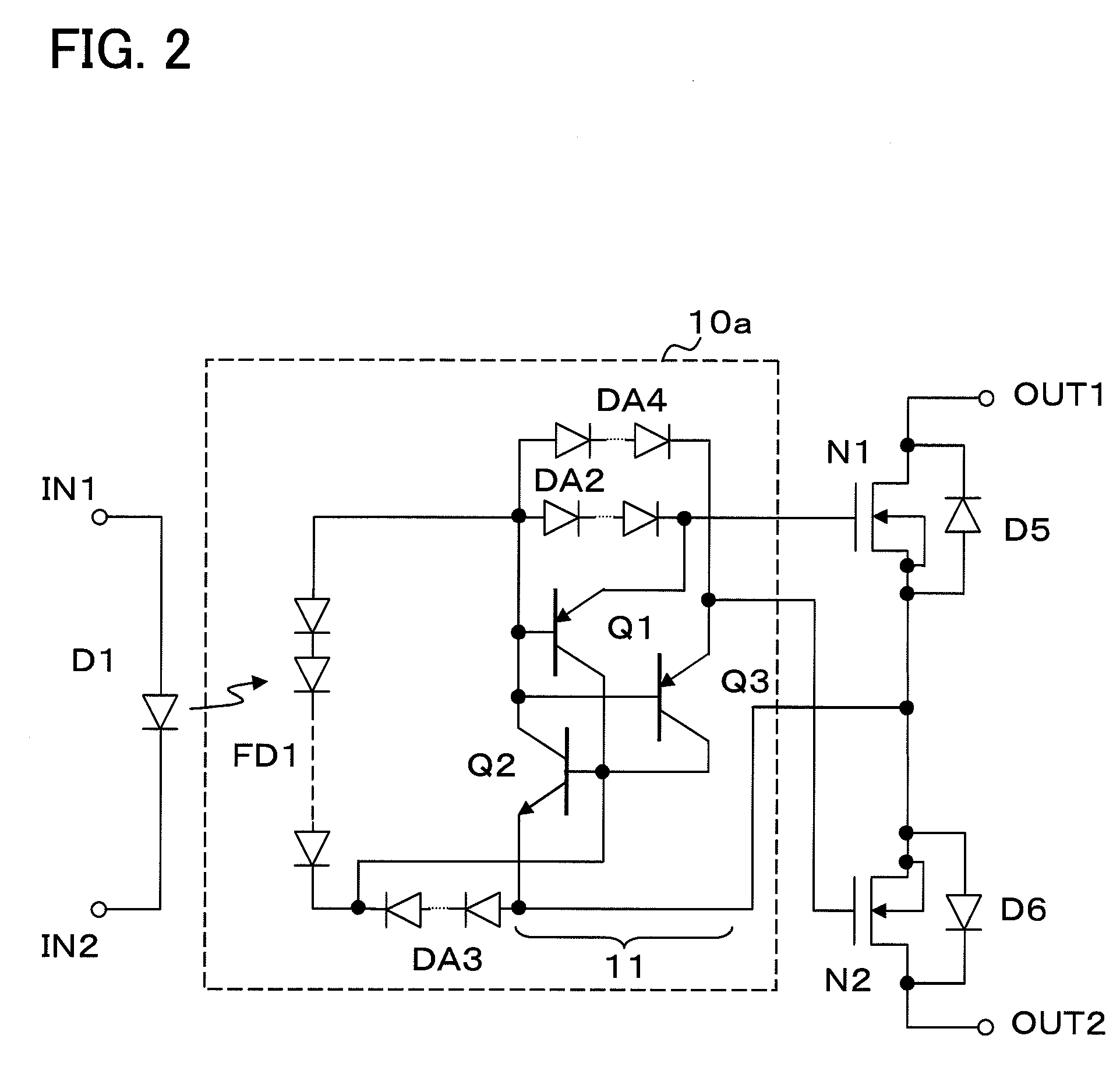
[0054]FIG. 2 is a circuit diagram of an optical semiconductor relay device according to a second example of the present invention. In FIG. 2, the symbols same as the ones in FIG. 1 indicate the same things, thus the explanations of them will be omitted. In the optical semiconductor relay device shown in FIG. 2, the diodes D2 to D4 are replaced by serially-connected diode arrays DA2 to DA4 respectively.

[0055]In the optical semiconductor relay device configured as above, since the diode arrays DA2 to DA4, in which a plurality of diodes are connected in series, are used as the diodes connected between the base and emitter electrodes of each transistor in the thyristors as the discharge circuits, the OFF capacitance (CPVD) of the drive circuit constituted by the photodiode array and the discharge circuit is reduced more than in the first example. As a result, it is possible to reduce the OFF capacitance (Cout2) between the output terminals even more.

[0056]FIG. 6 shows a variant of the c...


PUM


Abstract

A transient voltage occurring between output terminals during ON/OFF operation is reduced. There are provided a pair of input terminals IN1 and IN2, a pair of output terminals OUT1 and OUT2, MOSFETs N1 and N2 connected between the output terminals, and a drive circuit 10 connected between the input terminals IN1 and IN2 and the MOSFETs N1 and N2. A light-emitting diode D1 is connected between the input terminals IN1 and IN2. The MOSFETs N1 and N2 have their source electrodes electrically connected to each other and their drains connected to the output terminals OUT1 and OUT2 respectively. The drive circuit 10 includes a photodiode array FD1 that supplies a drive voltage to the gates of the MOSFETs N1 and N2, and a discharge circuit 11, connected between the gate electrodes and the source electrodes of the MOSFETs N1 and N2, that discharges electric charges accumulated on each gate electrode. (FIG. 1)

Description

REFERENCE TO RELATED APPLICATION[0001]This application is based upon and claims the benefit of the priority of Japanese patent application No. 2007-287459, filed on Nov. 05, 2007, the disclosure of which is incorporated herein in its entirety by reference thereto.FIELD OF THE INVENTION[0002]The present invention relates to an optical semiconductor relay device, and particularly to an optical semiconductor relay device comprising a plurality of MOSFETs between its output terminals.BACKGROUND OF THE INVENTION[0003]As semiconductor devices have increasingly higher capacitances and faster operation speeds, the test time of semiconductor testers that test these devices is also required to become faster. Further, it is crucial that the optical semiconductor relay in the tester has a low capacitance and high operation speed. As means for achieving low capacitance and high operation speed characteristics in an optical semiconductor relay, various optical semiconductor relay devices are prop...

Claims


Application Information

Patent Timeline
IPC IPC(8): H03K17/687H03K17/785
CPCH03K17/785H03K17/04206
Inventor MINAGAWA, TOMOHIRO
Owner RENESAS ELECTRONICS CORP
Why Eureka
Try Eureka