Double-layer super-junction Schottky diode

A diode and double-layer technology, applied in the field of double-layer superjunction Schottky diodes, can solve the problems of poor charge balance dynamic characteristics of superjunction power Schottky diodes

Inactive Publication Date: 2014-02-19
HARBIN ENG UNIV
View PDF2 Cites 5 Cited by
  • Summary
  • Abstract
  • Description
  • Claims
  • Application Information

AI Technical Summary

Problems solved by technology

[0006] In order to solve the above-mentioned problems about the charge balance and poor dynamic characteristics of super junction power Schottky diodes, the present invention proposes a double-layer super junction Schottky diode

Method used


Image

  • Double-layer super-junction Schottky diode
  • Double-layer super-junction Schottky diode
  • Double-layer super-junction Schottky diode

Examples


Embodiment Construction

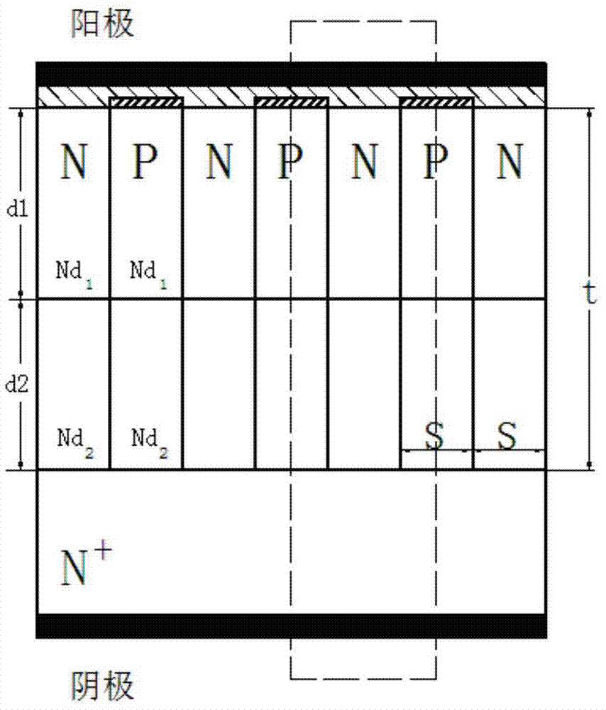
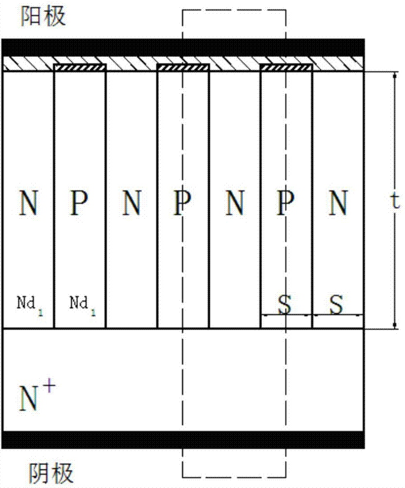
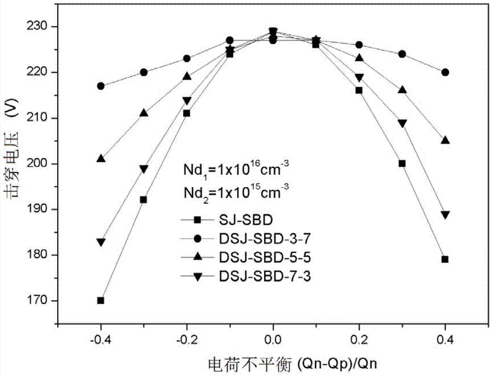
[0024] The technical solution of the embodiment of the present invention mainly includes: the drift region of the power Schottky device adopts a double-layer super junction structure, wherein the N column forms a Schottky contact with the metal anode, and the P column forms an ohmic contact with the metal anode. Wherein, the upper and lower double-layer superjunctions have the same width. The doping concentration of the upper superjunction is higher than that of the lower superjunction, and the depth and doping concentration of the upper and lower double-layer superjunctions are set in combination with the technical indicators of the actual power Schottky device.

[0025] Embodiments of the present invention will be described in detail below in conjunction with the accompanying drawings.

[0026] refer to figure 1 , the basic structure of the double-layer super junction Schottky diode (DSJ-SBD) of the present invention. DSJ-SBD adopts a double-layer superjunction structure, ...


PUM


Abstract

The invention discloses a double-layer super-junction Schottky diode. A double-layer super-junction structure is applied to a drift region of a power Schottky device. Due to the structure, on the premise that the forward characteristics of the device are not obviously lost, the relation between the reverse breakdown characteristic and charge imbalance of an ordinary super-junction Schottky diode is well improved, the reverse recovery characteristic of the device is greatly improved, the output capacitance of the device is reduced, and the power consumption of the device is effectively reduced.

Description

technical field [0001] The invention relates to the field of circuits, in particular to a double-layer superjunction Schottky diode. Background technique [0002] The super junction (SJ) theory first appeared in power MOSFETs, and it was proposed to break the "silicon limit". The silicon limit is a limit where the on-resistance is limited by the breakdown voltage. In 1988, D.J.Coe of Philips America Corporation proposed for the first time the method of using alternate pn structures in lateral high-voltage MOSFETs to replace low-doped drift regions in traditional power devices as voltage-resistant layers. In 1993, Professor Chen Xingbi of the University of Electronic Science and Technology of China proposed the method of using multiple pn structures as drift regions in vertical power devices, and called this structure "composite buffer layer". In 1995, J.Tihanyi of Siemens AG proposed a similar method. Since then, people began to pay attention to and study the superjunction...

Claims


Application Information

Patent Timeline
Patent Type & Authority Applications(China)
IPC IPC(8): H01L29/872
CPCH01L29/872H01L29/0634
Inventor 王颖徐立坤曹菲胡海帆
Owner HARBIN ENG UNIV
Why Eureka
Try Eureka