RF DMOS power device

A power device and radio frequency technology, applied in semiconductor devices, electrical components, circuits, etc., can solve the problem of increased capacitance in the depletion region, reduction in the width of the depletion layer, insufficient improvement in functional characteristic power gain, and additional power efficiency, etc. problem, to achieve the effect of reducing output capacitance, improving output characteristics, and high breakdown voltage

Inactive Publication Date: 2006-09-06
UNIV OF ELECTRONICS SCI & TECH OF CHINA
View PDF0 Cites 6 Cited by
  • Summary
  • Abstract
  • Description
  • Claims
  • Application Information

AI Technical Summary

Problems solved by technology

However, according to Gauss's theorem, the electric field of the buried oxide layer is three times that of silicon, so most of the vertical voltage drops to the buried oxide layer, which reduces the junction voltage under the buried oxide layer and reduces the width of the depletion layer below it. Small, so that the capacitance of the depletion region under the buried oxide layer increases
Therefore, its functional characteristics (including power gain, added power efficiency, etc.) have not been sufficiently improved

Method used


Image

  • RF DMOS power device
  • RF DMOS power device
  • RF DMOS power device

Examples


Embodiment Construction

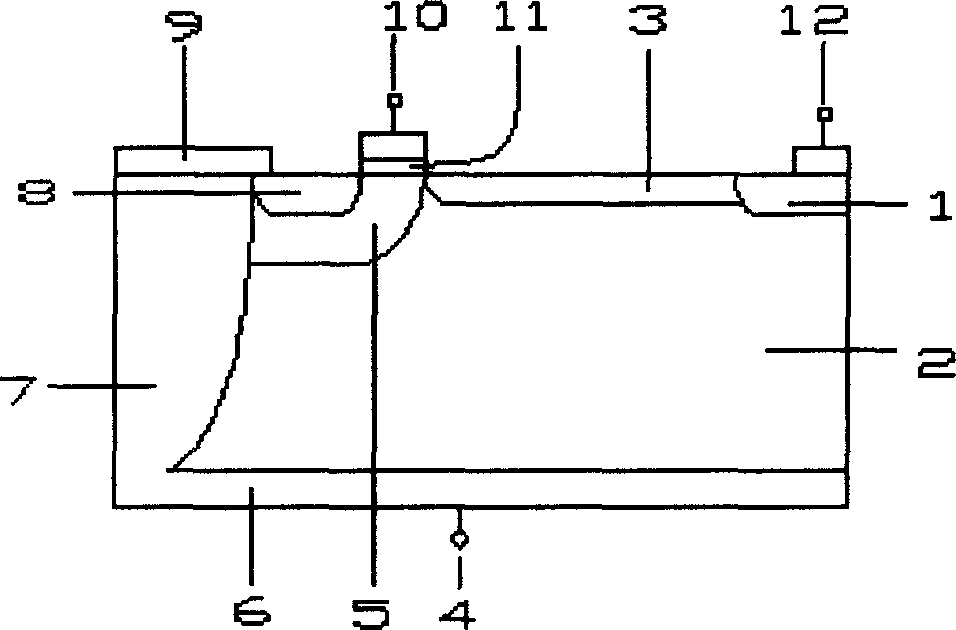
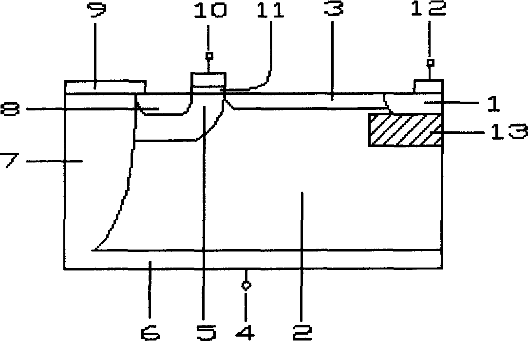
[0056] The part of the SOI / SON radio frequency DMOS power device with an n (or p) buried layer of the present invention has small output capacitance, good output characteristics and high withstand voltage. And this type of structure is compatible with radio frequency power integrated circuits.

[0057] In specific implementation, for some SOI radio frequency DMOS power devices with buried layers, an n (or p) buried layer can be deposited on the substrate first, then an epitaxial layer can be grown, and finally a silicon wafer can be partially oxidized using wafer bonding technology. Then, it is bonded with another silicon chip. The pre-oxygen implantation technology can also be used to implant oxygen into some areas of the silicon wafer to form a partial oxide insulating layer;

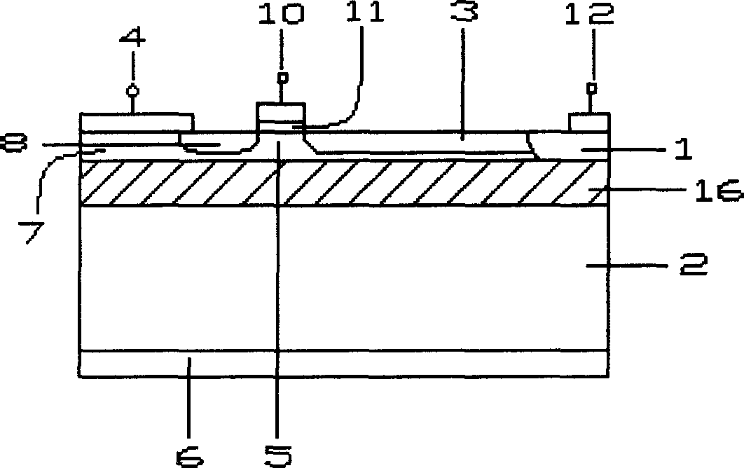
[0058] For some SON radio frequency DMOS power devices with buried layers, the n (or p) buried layer is also deposited on the substrate first, then the epitaxial layer is grown, and finally a wafer is par...


PUM


Abstract

RF DMOS power device belongs to semiconductor power device technology and RF integrated circuit technique field. It contains adding doped n or P) buried layer below site partial oxidation partial oxidation insulating layer in current part SOI RF DMOS power device, making part SOI RF DMOS device having buried layer, utilizing PN node principle to increase lower pole plate junction capacitance corresponded exhaustion width of drain region / epitaxial layer junction, wherewith to reduce output capacitance, thereby raising device output power, using part air space insulation layer substituting partial oxidation insulating layer also capable of making part SON RF DMOS device, utilizing interstice relative dielectric constant being 1 property to reduce device output capacitance and raise device output power, utilizing part air space insulation layer and low doped n (or P) buried layer to make part SON RF DMOS device having buried layer capable of preferable reducing device output capacitance and raising output power. Said invented device works on microwave band frequency, at the same time having higher pressure resistance, heat dispersion and frequency response performance.

Description

Technical field [0001] Radio frequency DMOS (DMOS: Double Diffused Metal Oxide Semiconductor) power devices belong to the field of semiconductor power device technology and radio frequency integrated circuit technology. Background technique [0002] Radio frequency DMOS power devices are widely used in narrow-band and high-gain wireless communication technologies. They have the following advantages: 1. The transconductance in the large current range remains large and constant, so the dynamic range of linear amplification is larger and larger. The output power can have a larger linear gain; second, the cross-modulation distortion is low; third, it can withstand high voltage, thereby increasing the output power of the device. [0003] In general LDMOS power devices, the drain, source and gate are all on the surface of the chip. Since the source is on the surface of the chip, it must be led out by an external lead, and the external lead of the source has a certain resistance and ind...

Claims


Application Information

Patent Timeline
Patent Type & Authority Applications(China)
IPC IPC(8): H01L29/78H01L29/36
Inventor 李泽宏王小松张波李肇基王一鸣王卓杨舰
Owner UNIV OF ELECTRONICS SCI & TECH OF CHINA
Why Eureka
Try Eureka