Three-dimensional semiconductor architecture

a semiconductor and three-dimensional technology, applied in semiconductor devices, semiconductor/solid-state device details, electrical devices, etc., can solve the problems of increasing the number of metallization layers, increasing so as to reduce the size of the overall device, and reduce the overall size limitation

Active Publication Date: 2013-10-08
TAIWAN SEMICON MFG CO LTD
View PDF64 Cites 21 Cited by
  • Summary
  • Abstract
  • Description
  • Claims
  • Application Information

AI Technical Summary

Benefits of technology

[0010]An advantage of embodiments of the present invention is that the number of metallization layers may be reduced, thereby leading to smaller overall devices. Additionally, overall size limitations may be reduced as signal and power connections may be relocated from the periphery of the device and placed into the interior of the substrate.

Problems solved by technology

However, due to routing congestion from the sheer number of contact pads, these contact pads are typically bunched together along the outside periphery of the device, which works to limit any reduction in the size of the overall device.
Further, as semiconductor devices have grown more powerful and more complicated, the internal routing interconnects within the metallization layers have also become more complicated.
This has resulted in an increase in the number of metallization layers, as well as an increase in resistivity and power consumption due to the extra layers high resistive vias that are required.
By requiring the signal, power, and ground connections to all be made through the contact pads over the metallization layer, the complexity and distance of the routing required for the power, ground, and signal interconnects is increased, leading to larger resistivities, larger power consumption, greater number of metallization layers, and larger overall production costs.

Method used


Image

  • Three-dimensional semiconductor architecture
  • Three-dimensional semiconductor architecture
  • Three-dimensional semiconductor architecture

Examples


Embodiment Construction

[0017]The making and using of embodiments of the present invention are discussed in detail below. It should be appreciated, however, that the present invention provides many applicable inventive concepts that can be embodied in a wide variety of specific contexts. The specific embodiments discussed are merely illustrative of specific ways to make and use the invention, and do not limit the scope of the invention.

[0018]The present invention will be described with respect to embodiments of the present invention in a specific context, namely a semiconductor die with I / O connections routed to the back side of the semiconductor die in a system-on-chip configuration. However, the present invention may also be used with other types of connections through a semiconductor die.

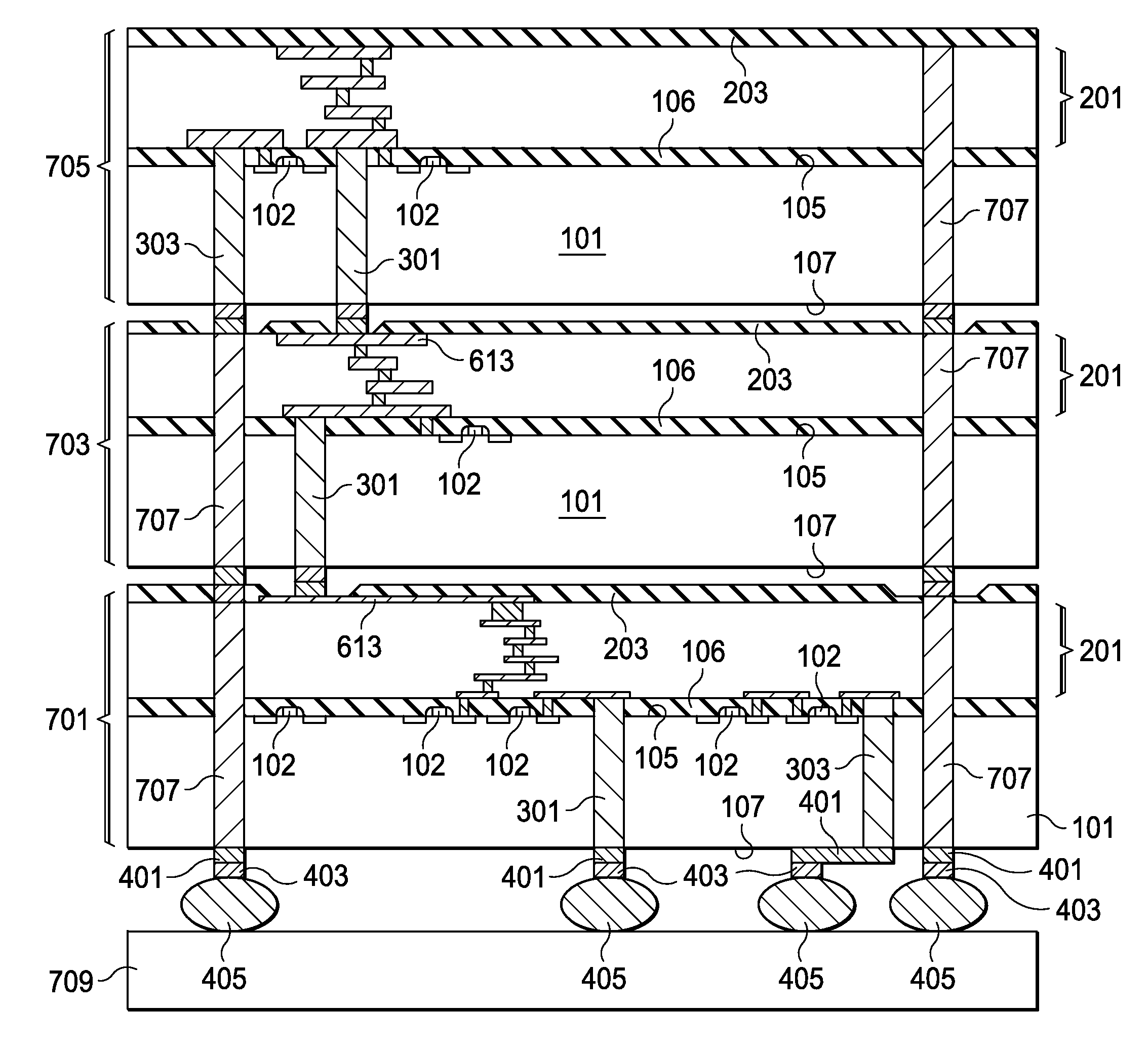
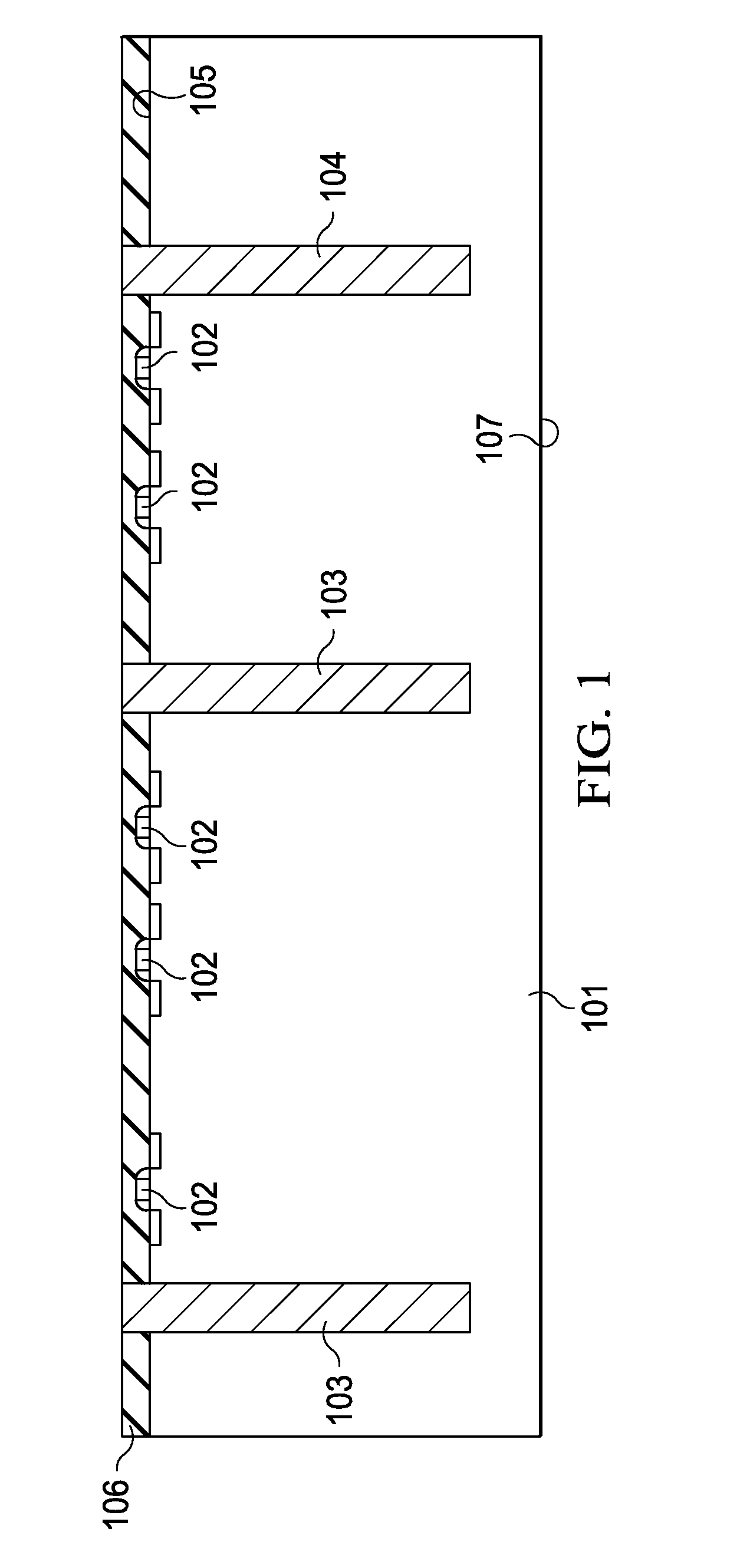
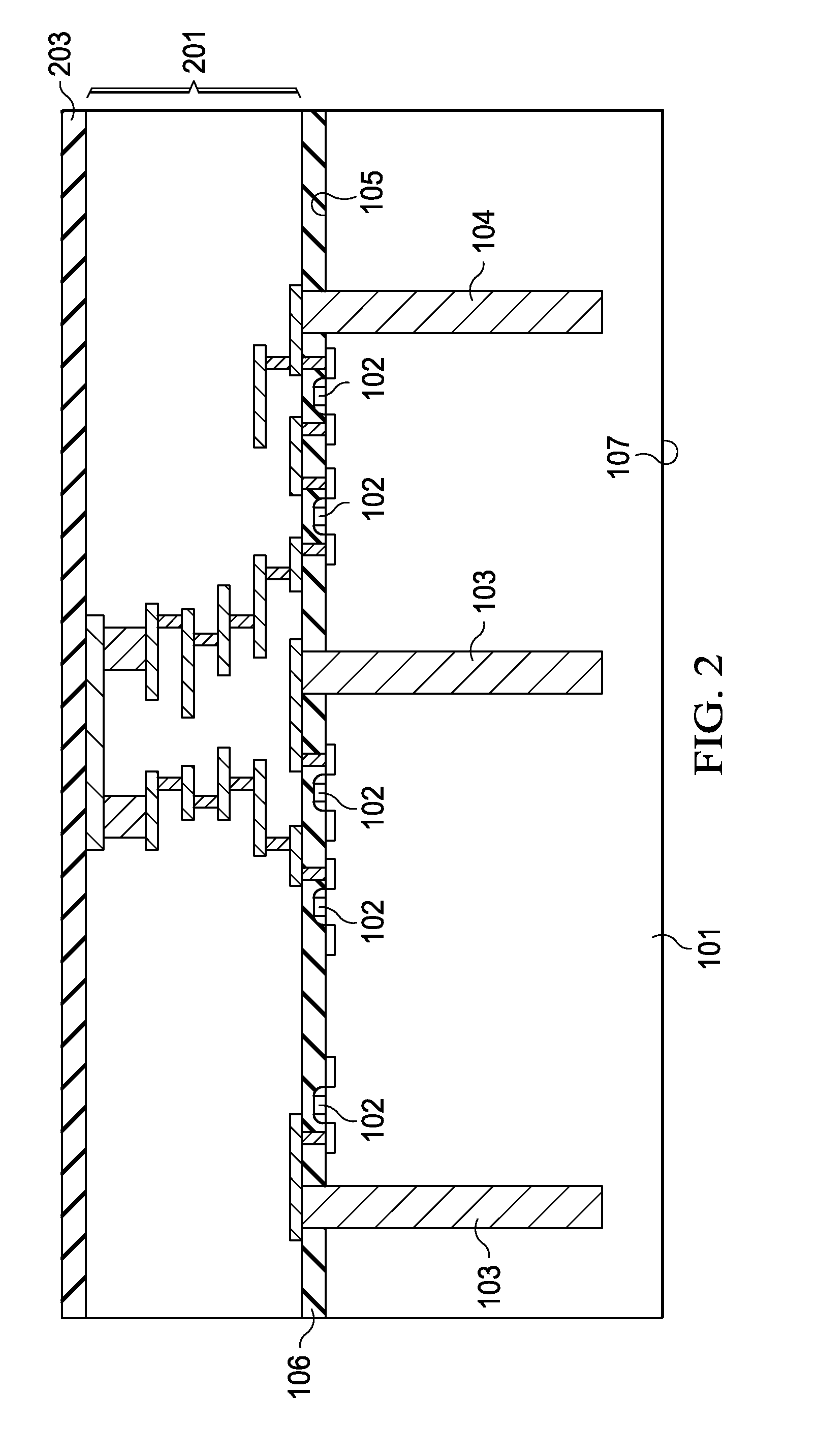
[0019]With reference now to FIG. 1, there is shown a substrate 101 with active devices 102 and an interlayer dielectric (ILD) 106, the substrate having a first side 105 and a second side 107 opposite the first side 105....


PUM


Abstract

A system and method for making semiconductor die connections with through-silicon vias (TSVs) are disclosed. TSVs are formed through the substrate to allow for signal connections as well as power and ground connections. In one embodiment this allows these connections to be made throughout the substrate instead of on the periphery of the substrate. In another embodiment, the TSVs are used as part of a power matrix to supply power and ground connections to the active devices and metallization layers through the substrate.

Description

[0001]This application claims the benefit of U.S. Provisional Patent Application Ser. No. 61 / 167,233, filed on Apr. 7, 2009, and entitled “Three-Dimensional Semiconductor Architecture,” which application is incorporated herein by reference.TECHNICAL FIELD[0002]The present invention relates generally to a system and method for connecting semiconductor devices and, more particularly, to a system and method for providing connections to a back side of a semiconductor die.BACKGROUND[0003]Generally, contact pads are used by semiconductor devices to provide for signal, power, and ground connectivity to exterior devices. Within the semiconductor devices the contact pads are generally connected to metallization layers located over the active devices. The metallization layers route the signal, power, and ground connections to their desired location, and also interconnect the various active devices in order to form functional circuitry.[0004]However, due to routing congestion from the sheer nu...

Claims


Application Information

Patent Timeline
Patent Type & Authority Patents(United States)
IPC IPC(8): H01L23/535
CPCH01L23/481H01L21/768H01L23/525H01L23/5286H01L24/05H01L24/10H01L24/13H01L25/0657H01L21/76877H01L23/49827H01L21/8221H01L2924/0002H01L2924/00014H01L2224/13009H01L2224/05009H01L24/16H01L24/17H01L27/0688H01L27/1203H01L2224/0401H01L2224/0557H01L2224/13025H01L2224/13099H01L2224/13111H01L2224/13139H01L2224/13147H01L2225/06513H01L2225/06541H01L2924/01013H01L2924/01014H01L2924/01015H01L2924/01022H01L2924/01029H01L2924/01032H01L2924/01033H01L2924/0105H01L2924/01073H01L2924/01074H01L2924/01078H01L2924/01079H01L2924/01082H01L2924/014H01L2924/04941H01L2924/04953H01L2924/14H01L2924/15311H01L2924/19041H01L2924/19042H01L2924/19043H01L2924/01006H01L2924/01019H01L2924/01024H01L2924/01047H01L2924/01075H01L2924/00H01L2224/05552H01L2224/16146H01L2224/13H01L2224/16145H01L21/76898H01L24/83
Inventor LAW, OSCAR M. K.WU, KUO H.
Owner TAIWAN SEMICON MFG CO LTD
Why Eureka
Try Eureka