Substrate processing apparatus

a processing apparatus and substrate technology, applied in the direction of coatings, chemical vapor deposition coatings, electric discharge tubes, etc., can solve the problems of difficult to define the length, film formed on a wafer, and reduced upper portion of the furnace, so as to reduce the vertical deformation of the electrodes

Active Publication Date: 2013-10-15
KOKUSA ELECTRIC CO LTD
View PDF13 Cites 1 Cited by
  • Summary
  • Abstract
  • Description
  • Claims
  • Application Information

AI Technical Summary

Benefits of technology

[0013]It is, therefore, a main object of the present invention to provide a substrate processing apparatus having electrodes which extend in a stacking direction of vertically stacked substrates and which are made of flexible member, the substrate processing apparatus being capable of reducing vertical deformation of the electrodes.

Problems solved by technology

Moreover, as shown in FIG. 13, since the length is different from one individual to another because a member having a knitted structure is extensible, i.e. the member under tension increases in length, it is difficult to define the length.
As a result, a thickness of a film formed on a wafer 200 located at the upper portion in the furnace is reduced, uniformity among the wafers is deteriorated, and a film forming result is deteriorated.

Method used


Image

  • Substrate processing apparatus
  • Substrate processing apparatus
  • Substrate processing apparatus

Examples


Embodiment Construction

[0030]Next, preferred embodiments of the present invention will be explained.

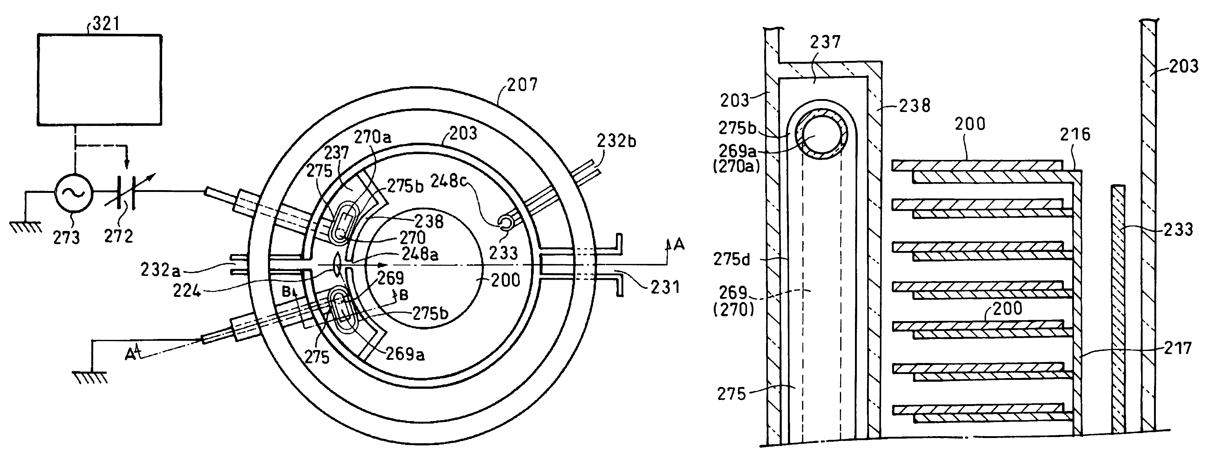
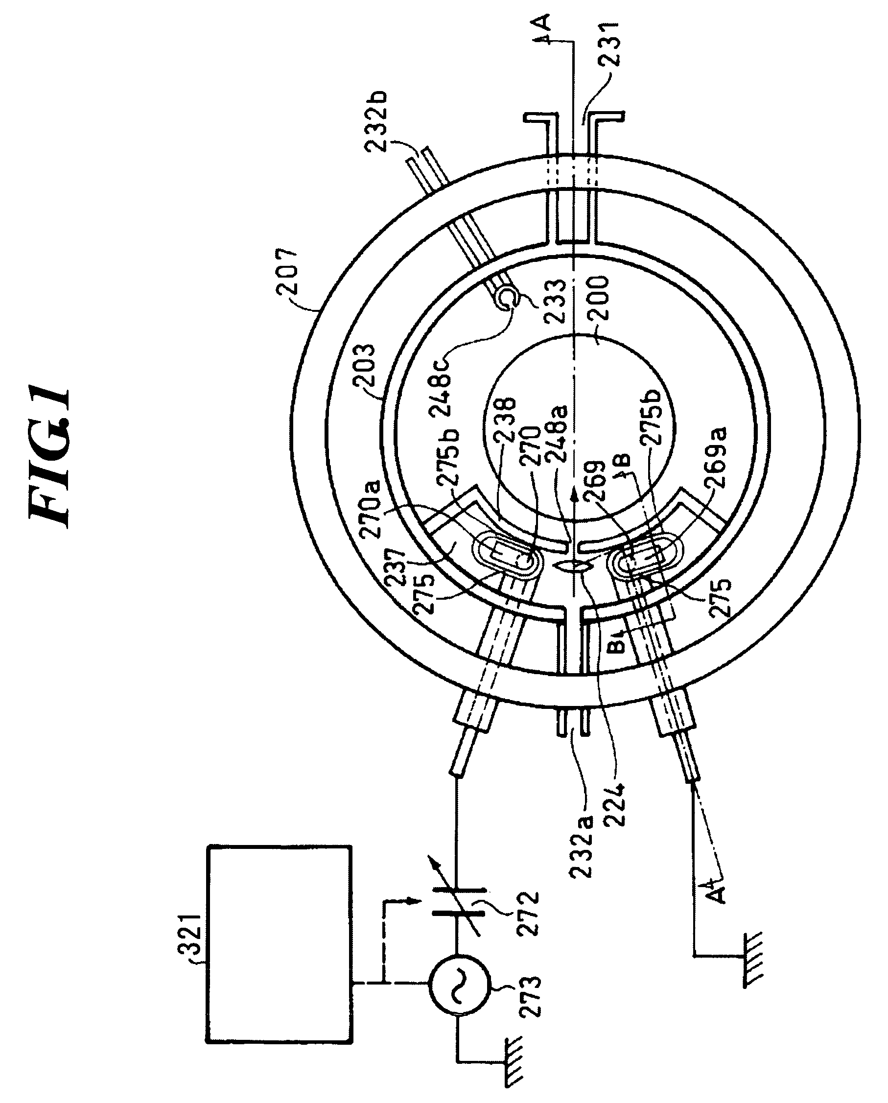
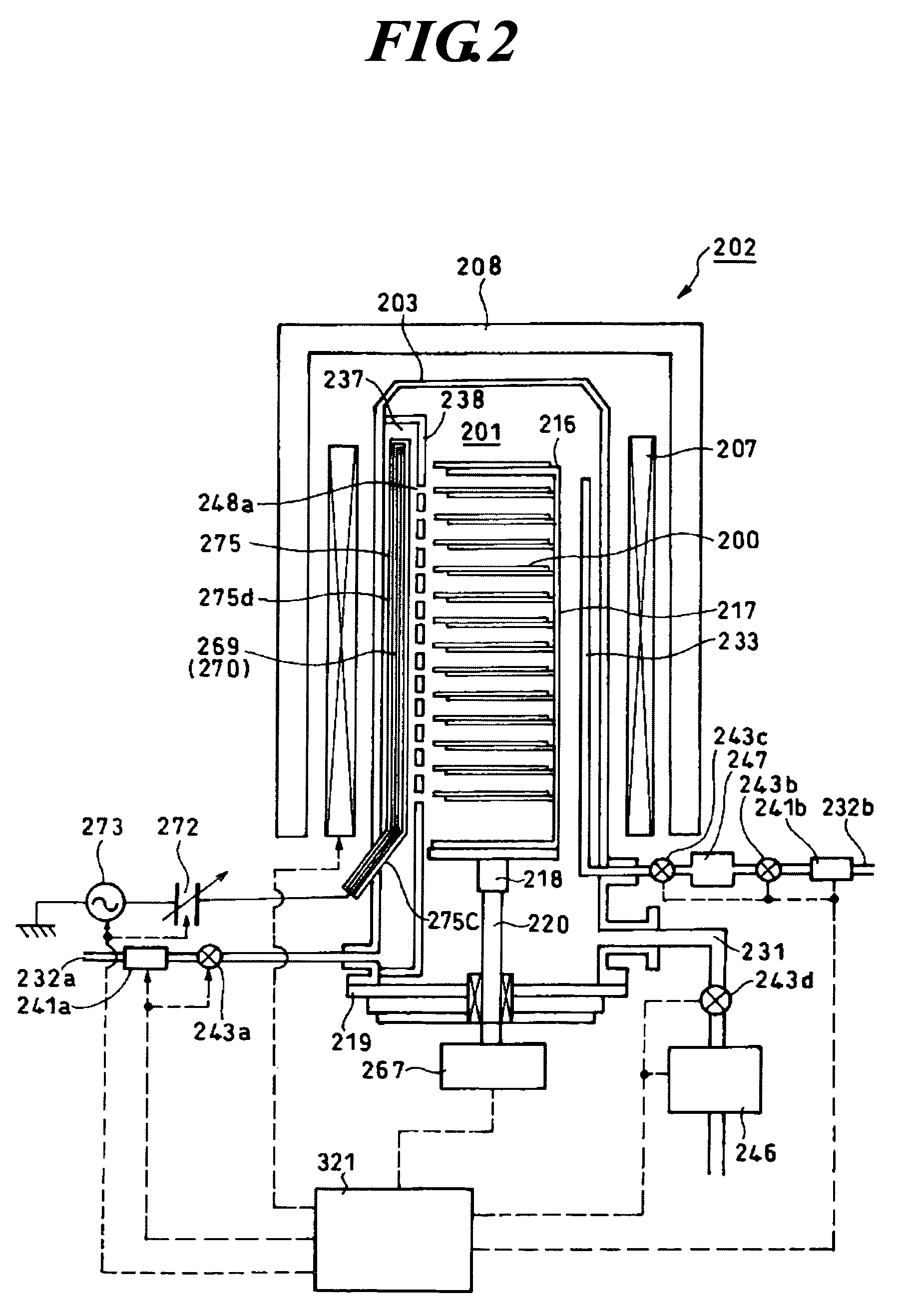
[0031]A vertical batch type semiconductor producing apparatus in the preferred embodiments of the present invention generates plasma to form a film on a wafer using braided electrodes accommodated in protecting tubes welded to an inner wall of a processing tube. Since each of the protecting tubes has at least one bent portion, friction between the inner wall of the protecting tube and the electrodes prevents the electrodes from being varied in shape.

[0032]Next, the preferred embodiments of the present invention will be explained in more detail with reference to the drawings.

[0033]In the embodiments, a film forming processing using an ALD (Atomic Layer Deposition) method as an example of processing on a substrate such as a wafer will be briefly explained.

[0034]According to the ALD method, two (or more) kinds of gases which are materials to be used for film formation are alternately supplied onto substrates o...


PUM

PropertyMeasurementUnit
temperatureaaaaaaaaaa
pressureaaaaaaaaaa
pressureaaaaaaaaaa

Abstract

Disclosed is a substrate processing apparatus, including: a processing chamber to accommodate a plurality of substrates therein in such a way that the substrate are vertically stacked; a gas supply system to supply processing gas into the processing chamber; an exhaust system to exhaust an atmosphere from the processing chamber; at least a pair of electrodes made of flexible member extending in a stacking direction of the substrates to activate the processing gas; and protecting tubes to accommodate the electrodes therein, wherein each of the protecting tubes is provided with a bent portion at a higher position than an uppermost substrate, and a tip end of each of the electrodes is located on a tip end side of each of the protecting tubes over the bent portion.

Description

BACKGROUND OF THE INVENTION[0001]1. Field of the Invention[0002]The present invention relates to a substrate processing apparatus, and more particularly, to a substrate processing apparatus which forms a film on a semiconductor wafer utilizing plasma-excited processing gas.[0003]2. Description of the Related Art[0004]FIG. 10 is a schematic transverse sectional view for explaining a vertical type substrate processing furnace of a conventional substrate processing apparatus. A vertical sectional view taken along the line C-C in FIG. 10 corresponds to a vertical sectional view in FIG. 2. FIG. 11 is an enlarged vertical sectional view taken along the line C-C in FIG. 10.[0005]Some substrate processing apparatuses which form a film on a semiconductor wafer utilizing plasma-excited processing gas have a structure that electrodes 269 and 270 for generating plasma are accommodated in electrode protecting tubes 275 in order to prevent a reaction with the processing gas.[0006]Each of the elec...

Claims


Application Information

Patent Timeline
Patent Type & Authority Patents(United States)
IPC IPC(8): C23C16/00
CPCC23C16/345C23C16/452C23C16/45542C23C16/4584C23C16/50C23C16/54H01J37/32009H01J37/32082H01J37/32541H01L21/3141H01L21/3185H01L21/0228H01L21/0217H01L21/20H01L21/22
Inventor YAMAMOTO, TETSUOKONTANI, TADASHI
Owner KOKUSA ELECTRIC CO LTD
Why Eureka
Try Eureka