Magnetic memory device and magnetic random access memory

a magnetic random access and memory technology, applied in the direction of magnetic field-controlled resistors, digital storage, instruments, etc., can solve the problems of increasing the area of the write operation, increasing the current consumption amount for the write operation, and the absolute value of the write current becomes relatively large, so as to achieve the effect of easy formation

Active Publication Date: 2013-10-15
NEC CORP
View PDF24 Cites 11 Cited by
  • Summary
  • Abstract
  • Description
  • Claims
  • Application Information

AI Technical Summary

Benefits of technology

[0031]A subject matter of the present invention is to provide a magnetic memory cell and a magnetic random access memory having a structure in which a magnetization fixed region can be formed easily, a pinning site of a domain wall can be formed easily, in an MRAM of a current drive domain wall motion type in which a magnetic anisotropy of a magnetization record layer is in a perpendicular direction.
[0035]According to the present invention, the magnetization fixed region can be easily formed and the pinning site of the domain wall can be easily formed.

Problems solved by technology

The chip area is necessarily increased when the write current is large, and also a current consumption amount increases for the write operation.
However, in the MRAM using a current drive domain wall motion, it is worried that an absolute value of the write current becomes relatively large.
As mentioned above, in the MRAM using the current drive domain wall motion, it is worried that the absolute value of the write current becomes relatively large.
However, when the magnetic anisotropy of the magnetization record layer is perpendicular as shown in FIG. 3A and FIG. 3B, and the magnetization is perpendicular to the in-plane direction, it is difficult to initialize with the external magnetic field even if the magnetization record layer is U-shaped.
Therefore, there is a possibility that the shape is deformed due to the manufacturing variation.
Moreover, it is very difficult to form the restricted section when the device is further miniaturized to make the width of the magnetization record layer narrow.
Also, there is a possibility that a work over the lithography limit of the semiconductor process is required.

Method used


Image

  • Magnetic memory device and magnetic random access memory
  • Magnetic memory device and magnetic random access memory
  • Magnetic memory device and magnetic random access memory

Examples


first exemplary embodiment

[0139]In a first exemplary embodiment, the magnetic memory cell and MRAM in a case of N=2 when will be described.

1. Basic Configuration of Magnetic Memory Device

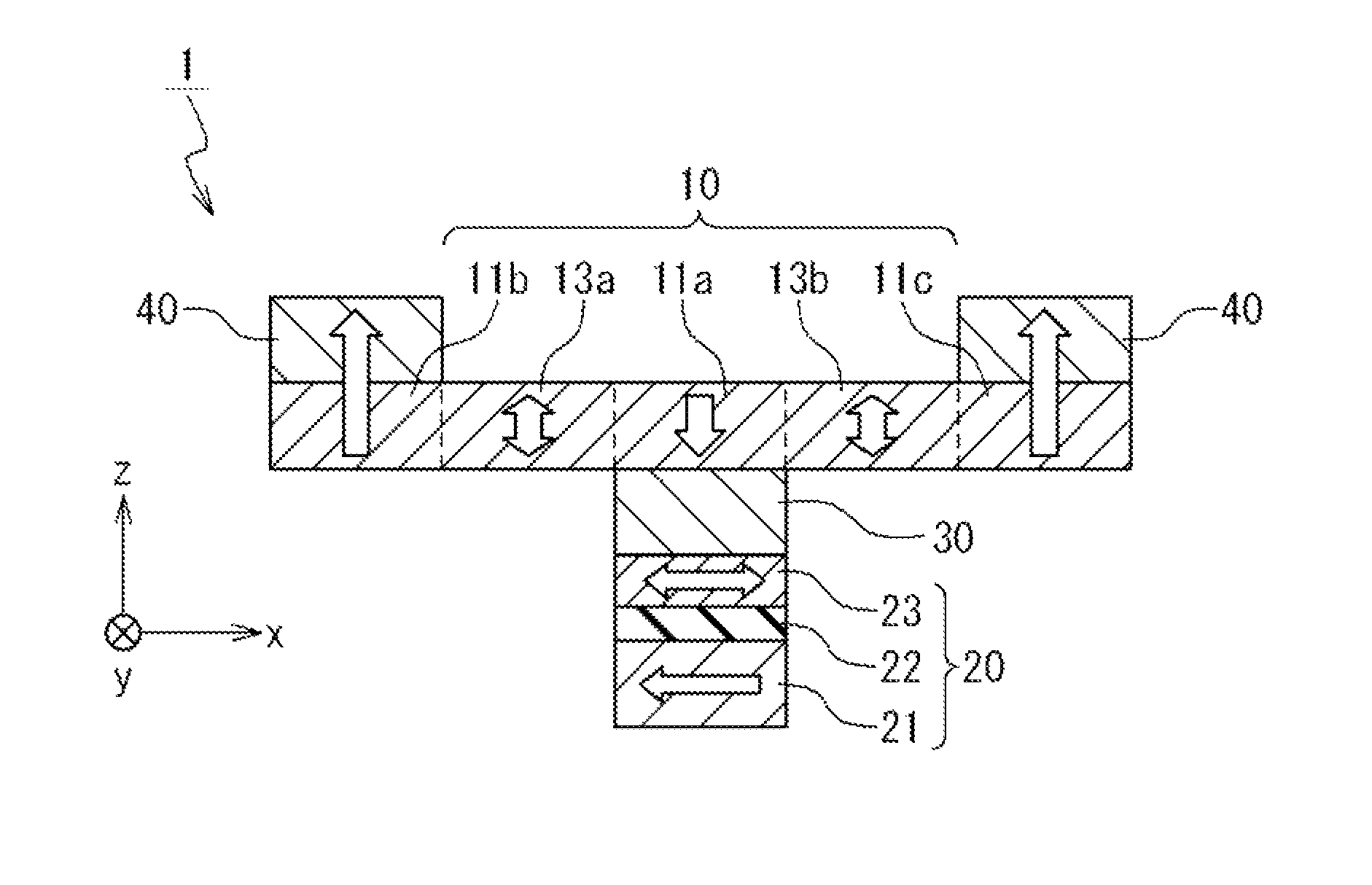
[0140]FIG. 4A is a plan view showing an example of the configuration of a magnetization record layer of a magnetic memory device according to the first exemplary embodiment of the present invention. FIG. 4B is a sectional view showing an example of the configuration of the magnetic memory device according to the first exemplary embodiment of the present invention. Here, in FIG. 4A and FIG. 4B, a mark of a white circle and a point, a mark of a white circle and a cross, and a white arrow show the magnetization direction of a concerned region, as used generally. Hereinafter, this is similarly applied to the specification and each drawing.

[0141]A magnetic memory device 1 is provided with a magnetization record layer 10 and a magnetic tunnel junction section 20. The magnetization record layer 10 is a ferromagnetic layer which has...

second exemplary embodiment

[0234]In a second exemplary embodiment, the magnetic memory cell and the MRAM in a case of N=2 will be described.

1. Basic Configuration of Magnetic Memory Device

[0235]FIG. 24 is a plan view showing an example of the configuration of the magnetization record layer of the magnetic memory device according to the second exemplary embodiment of the present invention. The magnetic memory device 1 in the present exemplary embodiment is provided with the magnetization record layer 10 and the magnetic tunnel junction section 20, and is basically the same as the magnetic memory device I in the first exemplary embodiment. Here, the present exemplary embodiment differs from the first exemplary embodiment in that an auxiliary magnetization fixed region 11a2 is connected to the 0th magnetization fixed region 11a. The auxiliary magnetization fixed region 11a2 is formed of the same material as the 0th magnetization fixed region 11a, has the same perpendicular magnetization anisotropy and is magneti...

modification example

11. Modification Example

[0260]FIG. 30 is a plan view showing the configuration of the magnetization record layer of the magnetic memory device according to a modification of the second exemplary embodiment of the present invention. In the configuration of the magnetization record layer of FIG. 24, the auxiliary magnetization fixed region 11a2 is connected with the 0th magnetization fixed region 11a, and the current supply terminal 53 is connected with the auxiliary magnetization fixed region 11a2. However, the present invention is not limited to this example, and as shown in FIG. 30, the current supply terminal 53 may be directly connected with the 0th magnetization fixed region 11a without passing through the auxiliary magnetization fixed region 11a2. In this case, the magnetic anisotropy of the sensor layer 23 needs to turn to the direction of ±y.

[0261]Because the remaining portion of the configuration and the operations is same as that mentioned previously, the description is omi...


PUM


Abstract

A magnetic memory cell is provided with a magnetization record layer and a magnetic tunnel junction section. The magnetization record layer is a ferromagnetic layer having a perpendicular magnetic anisotropy. The magnetic tunnel junction section is used to read data from the magnetization record layer. The magnetization record layer has a plurality of domain wall motion regions.

Description

[0001]This patent application is the National Phase of PCT / JP2009 / 071410, filed Dec. 24, 2009, which claims priorities on convention based on Japanese Patent Application No. 2008-330508 filed on Dec. 25, 2008 and Japanese Patent Application No. 2009-229597 filed on Oct. 1, 2009. The disclosures thereof are incorporated herein by reference.TECHNICAL FIELD[0002]The present invention is related to a magnetic memory device and a magnetic random access memory, and more particular to a domain wall motion-type magnetic memory device and a magnetic random access memory.RELATED ART[0003]The magnetic random access memory (MRAM) is expected to be a non-volatile memory device that a high-speed operation is possible, and an infinite rewrite operation is possible, and the research extensively progresses. In the MRAM, magneto-resistance elements are integrated in a memory cell and data is stored based on the magnetization direction of a ferromagnetic layer of the magneto-resistance element. Some p...

Claims


Application Information

Patent Timeline
Patent Type & Authority Patents(United States)
IPC IPC(8): G11C11/00
CPCG11C11/14G11C11/5607G11C19/0808G11C19/0841H01L43/08H01L27/228G11C11/1655G11C11/1659G11C11/1675G11C11/1673G11C11/161H10B61/22H10N50/10
Inventor FUKAMI, SHUNSUKENAGAHARA, KIYOKAZUSUZUKI, TETSUHIROISHIWATA, NOBUYUKIOHSHIMA, NORIKAZU
Owner NEC CORP
Why Eureka
Try Eureka