
Self-aligned trench contact and local interconnect with replacement gate process

a technology of trench contacts and replacement gate structures, which is applied in the direction of semiconductor/solid-state device manufacturing, semiconductor devices, electrical apparatus, etc., can solve the problems of difficult bidirectional local interconnection patterning, easy failure of misalignment, and most replacement gate processes that are not self-aligned, etc., to reduce the number of resistive interfaces, improve manufacturing yield, and reduce the potential for misalignment

Active Publication Date: 2013-10-22
ADVANCED MICRO DEVICES INC
View PDF14 Cites 16 Cited by
  • Summary
  • Abstract
  • Description
  • Claims
  • Application Information

AI Technical Summary

Benefits of technology

This patent describes a new process for making semiconductors more efficiently. By using a special technique, the contacts that connect to the semiconductor can be aligned with the gate, making it simpler and more accurate. This process also reduces the capacitance between the connections, leading to better performance and fewer failures. Overall, this patent provides a better way to make semiconductors more reliably and efficiently.

Problems solved by technology

Additionally, most replacement gate processes suffer from alignment issues when making trench contacts and / or local interconnect connections to the gate.
For example, most replacement gate processes are not self-aligned and can easily fail from misalignment during processing.
It may also be difficult to pattern bidirectional local interconnect and / or reduce the number of interface layers from the local interconnect to either the gate or the source / drain of the gate.
Such process flows, however, are typically very complex, have many resistive interfaces, and have high manufacturing costs due to the complex process flow.
Additionally, there is a low manufacturing margin for misalignments or other errors due to the complexity of the processes as these processes may have severely restrictive design and / or alignment rules.
In addition, there may easily be alignment issues between local interconnect 68C and gate 56′ without restrictive alignment rules.
The numerous process steps may increase the likelihood of resistive interfaces forming between the local interconnects and / or alignment issues between the local interconnects.

Method used


Image

  • Self-aligned trench contact and local interconnect with replacement gate process
  • Self-aligned trench contact and local interconnect with replacement gate process
  • Self-aligned trench contact and local interconnect with replacement gate process

Examples


Embodiment Construction

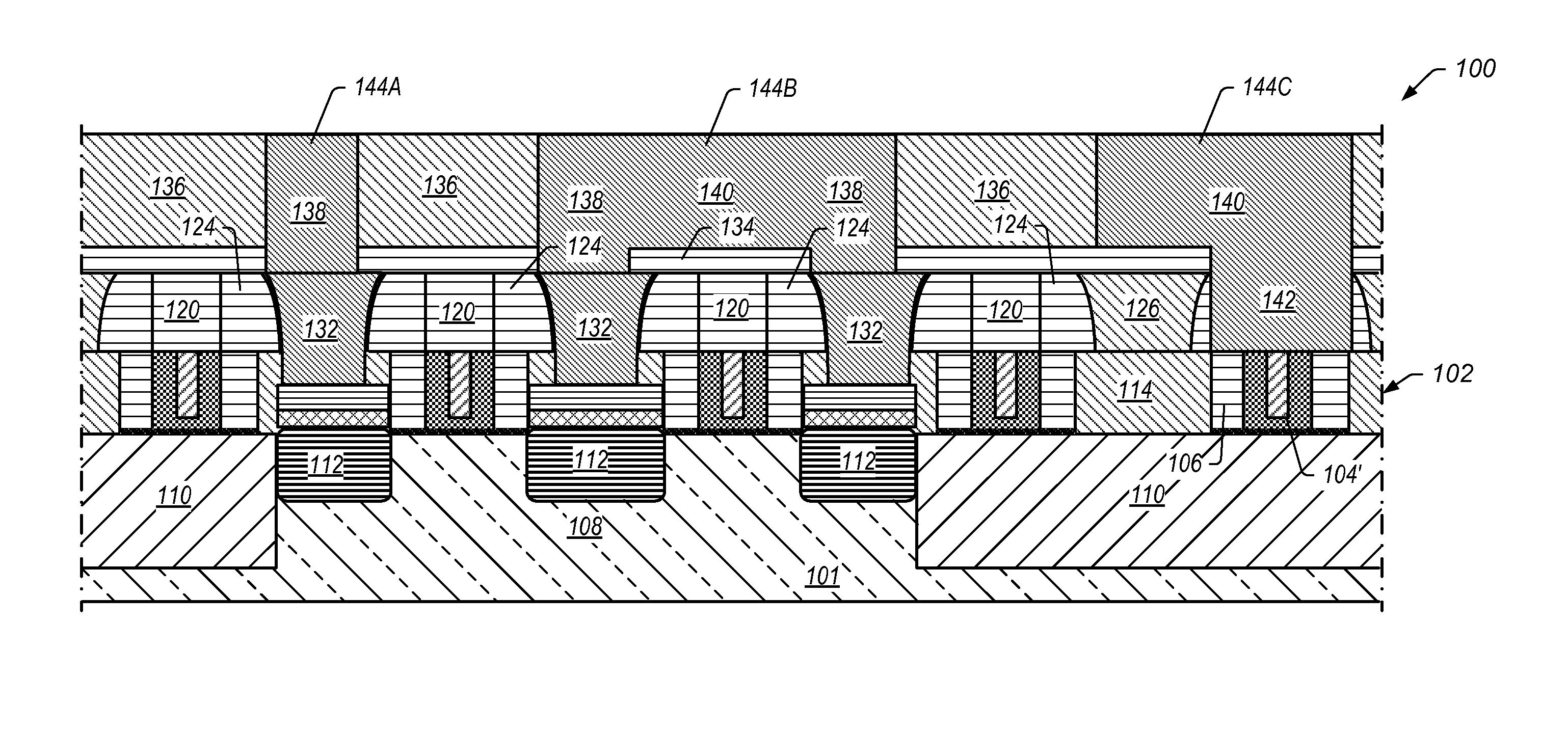
[0013]In certain embodiments, a semiconductor device fabrication process includes providing a transistor with one or more replacement metal gates on a semiconductor substrate. The transistor includes gate spacers of a first insulating material around each gate and a first insulating layer of a second insulating material between the gates and gate spacers. At least some of the second insulating material overlies sources and drains of the gates.

[0014]One or more insulating mandrels are formed and aligned over the gates. The insulating mandrels include the first insulating material. Each insulating mandrel has approximately the same width as its underlying gate with each mandrel being at least as wide as its underlying gate. Mandrel spacers are formed around each insulating mandrel. The mandrel spacers include the first insulating material. Each mandrel spacer has a profile that slopes from being wider at the bottom to narrower at the top.

[0015]A second insulating layer of the second i...


PUM


Abstract

A semiconductor device fabrication process includes forming insulating mandrels over one or more replacement metal gates on a semiconductor substrate. The mandrels include a first insulating material. Each mandrel has approximately the same width as its underlying gate with each mandrel being at least as wide as its underlying gate. Mandrel spacers are formed around each insulating mandrel. The mandrel spacers include the first insulating material. Each mandrel spacer has a profile that slopes from being wider at the bottom to narrower at the top. A second insulating layer of the second insulating material is formed over the transistor. Trenches to the sources and drains of the gates are formed by removing the second insulating material from portions of the transistor between the mandrels. Trench contacts to the sources and drains of the gates are formed by depositing conductive material in the first trenches.

Description

BACKGROUND OF THE INVENTION[0001]1. Field of the Invention[0002]This invention relates generally to semiconductor processes for forming transistors and, more specifically, to processes for forming trench contacts and local interconnects to a replacement gate structure on a semiconductor substrate.[0003]2. Description of the Related Art[0004]Transistors such as planar transistors have been the core of integrated circuits for several decades. During the use of transistors, the size of the individual transistors has steadily decreased through advances in process development and the need to increase feature density. Current scaling employs 32 nm technologies with development also progressing towards 20 nm and beyond technologies (e.g., 15 nm technologies).[0005]Replacement gate processes (flows) are becoming more commonly utilized as they avoid certain problems found in gate first processes. For example, replacement gate processes may avoid problems associated with the stability of the ...

Claims


Application Information

Patent Timeline
Patent Type & Authority Patents(United States)
IPC IPC(8): H01L29/94H01L31/062H01L31/113H01L31/119
CPCH01L21/76895H01L21/76897H01L29/66545H01L21/76832
Inventor SCHULTZ, RICHARD T.
Owner ADVANCED MICRO DEVICES INC
Learn More