Radiation detection and a method of manufacturing a radiation detector

a radiation detector and manufacturing method technology, applied in the direction of instruments, x/gamma/cosmic radiation measurement, semiconductor devices, etc., can solve the problems of deteriorating energy resolution, inter-pixel crosstalk, and high cost of cd(zn)te, so as to reduce crosstalk and manufacture the radiation detector cheap and simple

Active Publication Date: 2013-10-22
KONINKLIJKE PHILIPS ELECTRONICS NV
View PDF21 Cites 5 Cited by
  • Summary
  • Abstract
  • Description
  • Claims
  • Application Information

AI Technical Summary

Benefits of technology

[0006]This object is achieved by providing a trench in the semiconductor material which trench surrounds each pixel and is at least partly filled with a barrier material that absorbs at least a part of the photons generated by the incident radiation. Thus the trench, surrounding each pixel, has the property that it is able to absorb a part of the radiation generated photons, thereby reducing the crosstalk scattering of the incident radiation between the pixels. In this way the amount of radiation crosstalk that enters from a pixel into an adjacent pixel is reduced. Furthermore, the trench can be integrated in a simple way in a standard semiconductor process for manufacturing the radiation detector according to the invention. For example, a CMOS (Complementary Metal Oxide Semiconductor) process for the manufacture of the radiation detector according to the invention provides for a simple and cheap manufacturing of the radiation detector according to the invention in which the manufacturing of the trench is integrated in a simple way. Advantageously the semiconductor material comprises silicon for which standard and cheap manufacturing processes are available.
[0007]In an embodiment of the radiation detector according to the invention, each pixel comprises an array of sub-pixels and each sub-pixel is surrounded by the trench. This further reduces the amount of crosstalk in the radiation detector. In another embodiment a cluster of adjacent sub-pixels is surrounded by the trench. This allows for an optimization of the size of the active area of the sub-pixels and reduction of the cross-talk, because the trench occupies an area which reduces the active area of the pixels and sub-pixels but on the other hand reduces the cross-talk. This, for example, allows for an increased coverage of the active area of the array of sub-pixels at the cost of accepting some spatial crosstalk between sub-pixels of the array.
[0008]In an embodiment of the radiation detector according to the invention, the barrier material comprises a material which does not show K fluorescence above an energy of 35 keV. Thus undesired crosstalk effects can be minimized.
[0009]In an embodiment of the radiation detector according to the invention, the filling factor of the barrier material in the trench varies programmably across the detector. In this way it is achieved that a first portion of the trench has a filling factor or filling volume of the barrier material that is different from the filling factor or filling volume of a second portion of the trench. For example, the first portion of the trench surrounds a pixel and the second portion of the trench surrounds a sub-pixel or a cluster of sub-pixels. This advantageously provides for optimization between the material used for filling, the size of the trench and the resulting quality of the filling process.
[0011]In an embodiment of the radiation detector according to the invention, the trench has a depth in the conversion layer in the range between 20 μm and 600 μm. This provides for a depth of the trench that corresponds to the maximum depth that the photons penetrate into the layer of the semiconductor material, thereby minimizing the cross-talk.
[0012]The object is also achieved by a method of manufacturing the radiation detector according to the invention in which the trench is provided in a substrate of a semiconductor material after which the surfaces of the trench are covered with an isolation layer. Thereafter an array of pixels is manufactured on the substrate whereby each pixel is surrounded by the trench. Finally, the trench is at least partly filled with a barrier material that absorbs at least a part of the photons generated by the incident radiation. The steps that are required for providing the trench and the at least partly filling of the trench are all processing steps that can be integrated in a standard semiconductor manufacturing process, thus resulting in a cheap and simple manufacturing of the radiation detector according to the invention.

Problems solved by technology

Although Cd(Zn)Te has a much higher stopping power than silicon and exhibits much less Compton scatter resulting in inter-pixel crosstalk, Cd(Zn)Te shows significant K-fluorescence, which deteriorates the energy resolution and can also cause inter-pixel crosstalk.
Furthermore, Cd(Zn)Te is an expensive material, difficult to manufacture in large sizes and, due to its brittleness, exhibits limitations as to layer thicknesses.
However, for medium photon energies a high probability for Compton scatter exists, which alters the photon direction as well as its energy, giving rise to spatial and spectral crosstalk between neighbouring and further away pixels.
One major disadvantage of such a semiconductor based radiation detector is the amount of crosstalk between pixels, mainly due to Compton scatter, that reduces the image quality.
A disadvantage of this radiation detector is that only cross-talk is reduced between adjacent radiation detectors and not between the pixels of each radiation detector.
Furthermore, it requires a complicated fabrication process in which the radiation detectors are mounted on a collimator board that reduces the crosstalk between the radiation detectors.

Method used


Image

  • Radiation detection and a method of manufacturing a radiation detector
  • Radiation detection and a method of manufacturing a radiation detector
  • Radiation detection and a method of manufacturing a radiation detector

Examples


Embodiment Construction

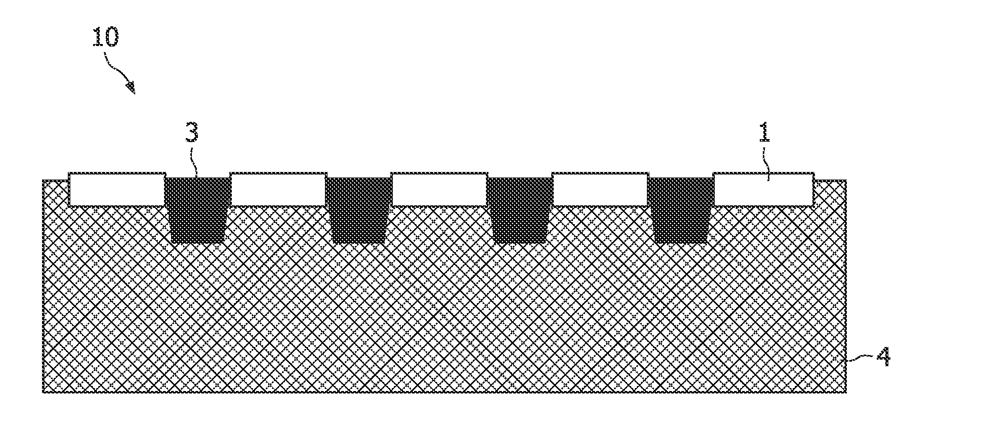
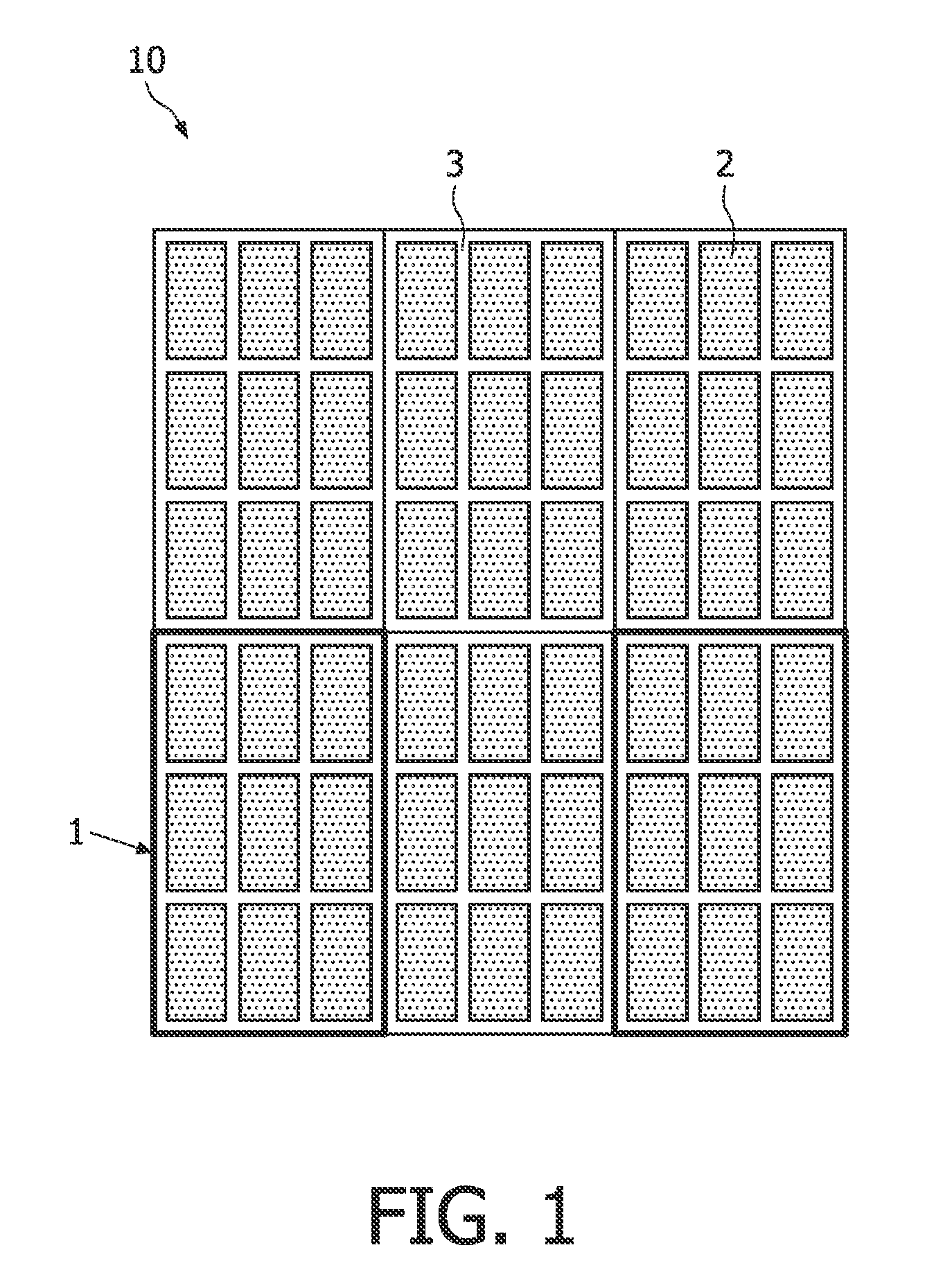
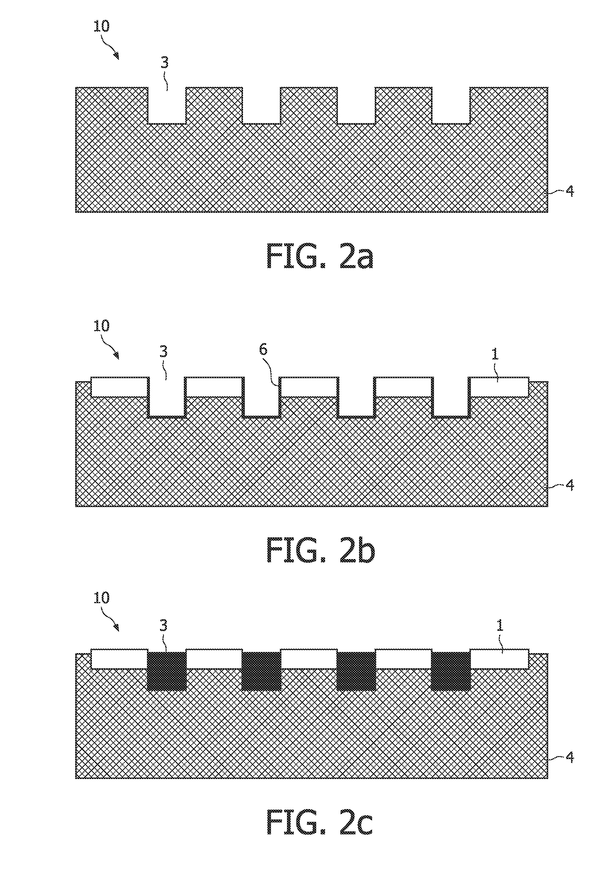
[0024]“Spectral CT” is considered to have the potential of revolutionizing present CT systems in such a way that spectral information contained in the poly-chromatic X-ray beam generated by an X-ray tube and passing a scanned object is used to provide new and diagnostically critical information. The enabling technology for Spectral CT imaging systems is a detector which can provide a sufficiently accurate estimate of the energy spectrum of the photons hitting the detector behind the scanned object. Since for image reconstruction reasons the detector is also exposed to the direct beam, the photon count rates in a detector pixel seeing the direct beam are huge (approximately 109 photons per mm2 and second, i.e. 1000 Mcps per mm2). Readout electronics are however expected to be able to cope with not more than 10 Mcps. To limit the counting rates, it is possible to sub-structure the sensor part of a detector (in which an X-ray photon interacts and generates a charge pulse, which is furt...


PUM


Abstract

The invention relates to a radiation detector (10), comprising an array of pixels (1), wherein each pixel (1) comprises a conversion layer of a semiconductor material (4) for converting incident radiation into electrical signals and wherein each pixel (1) is surrounded by a trench (3) that is at least partly filled with a barrier material that absorbs at least a part of photons generated by the incident radiation. The invention also relates to a method of manufacturing such a radiation detector (10).

Description

FIELD OF THE INVENTION[0001]The invention relates to a radiation detector and a method of manufacturing a radiation detector. Moreover, it relates to an X-ray detector and an imaging system comprising such a radiation detector.BACKGROUND OF THE INVENTION[0002]Radiation detectors, having an array of pixels, are applied in, for example, CT imaging systems, to provide a sufficiently accurate measure of the radiation incident on the detector after it has left a scanned object. The use of easy to manufacture semiconductor material, such as silicon, for the radiation detector is beneficial in view of for example costs, compared to, for example, Cd(Zn)Te as a sensor material. Although Cd(Zn)Te has a much higher stopping power than silicon and exhibits much less Compton scatter resulting in inter-pixel crosstalk, Cd(Zn)Te shows significant K-fluorescence, which deteriorates the energy resolution and can also cause inter-pixel crosstalk. Furthermore, Cd(Zn)Te is an expensive material, diffic...

Claims


Application Information

Patent Timeline
Patent Type & Authority Patents(United States)
IPC IPC(8): H01L31/115H01L21/00
CPCG01T1/2928
Inventor VOGTMEIER, GEREONHERRMANN, CHRISTOPHENGEL, KLAUS JUERGEN
Owner KONINKLIJKE PHILIPS ELECTRONICS NV
Why Eureka
Try Eureka