Transition metal oxide bilayers

a metal oxide bilayer and transition metal oxide technology, applied in the direction of bulk negative resistance effect devices, electrical equipment, semiconductor devices, etc., can solve the problem of limiting the areal density of a reram memory array based on the devi

Active Publication Date: 2013-10-29
SANDISK TECH LLC +2
View PDF1 Cites 27 Cited by
  • Summary
  • Abstract
  • Description
  • Claims
  • Application Information

AI Technical Summary

Problems solved by technology

However, the relatively thick structures disclosed by Lee would limit the areal density of a ReRAM memory array based on the devices.

Method used


Image

  • Transition metal oxide bilayers
  • Transition metal oxide bilayers
  • Transition metal oxide bilayers

Examples


example 1

Sub-Oxide Compositional Analysis

[0079]Tantalum oxide layers of varying composition were made by dc reactive sputtering in a locally built chamber as described above using either 4.3% or 5.4% O2 in Ar (generally at 1-5 mTorr and 100-300 W). (All relative concentrations are set as volume flow rates such as standard cubic centimeters per minute [sccm].) These layers were expected to have substoichiometric composition. The layers were analyzed using XPS. The spectra of two samples are shown in FIGS. 11A and B, respectively, together with the peaks associated with a least-squares fit of possible constituents. The overall fit to the data is very good. Table 1 summarizes the compositional analysis:

[0080]

TABLE 1% O2 in Ar carrier gas% Ta2O5% TaO2% TaO4.3831075.486 86

[0081]The presence of TaO2 and TaO sub-oxides was confirmed. It is also apparent that the amount of sub-oxide present in the deposited layer can be tuned by adjusting the O2 concentration in the carrier gas.

[0082]Three additiona...

example 2

Deep UV Spectral Ellipsometry Measurements

[0085]The samples described in Example 1 were further analyzed using deep UV spectral ellipsometry. Each sample was analyzed before and after annealing for 1 min at 750 C in an Ar / H2 atmosphere. The results are shown in FIGS. 12A and B and 13A-D. ‘n’ and ‘k’ are the refractive index and extinction coefficient respectively.

[0086]As can be seen in the figures, the samples made with O2 concentrations below 10% show significant absorption at lower energies, indicative of metallic or low band-gap suboxide phases. These are reduced but not eliminated after anneal. At higher O2 concentrations these lower energy absorptions are absent.

example 3

Deposition Rate

[0087]In order to controllably manufacture the very thin layers (several atomic thicknesses) required to make the near-stoichiometric Ta2O5-δ resistive switching layer, one must be able to provide a suitably slow deposition rate so that thickness can be controlled by process time. FIG. 14 shows that such control is indeed possible. The data are for 100 W power in a dc reactive sputtering process as a function of the O2 concentration in the Ar / O2 atmosphere. While the deposition rate for the lower O2 concentrations is significantly higher than for higher concentrations, all rates are acceptably low to allow precise thickness control.


PUM


Abstract

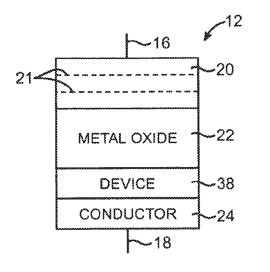
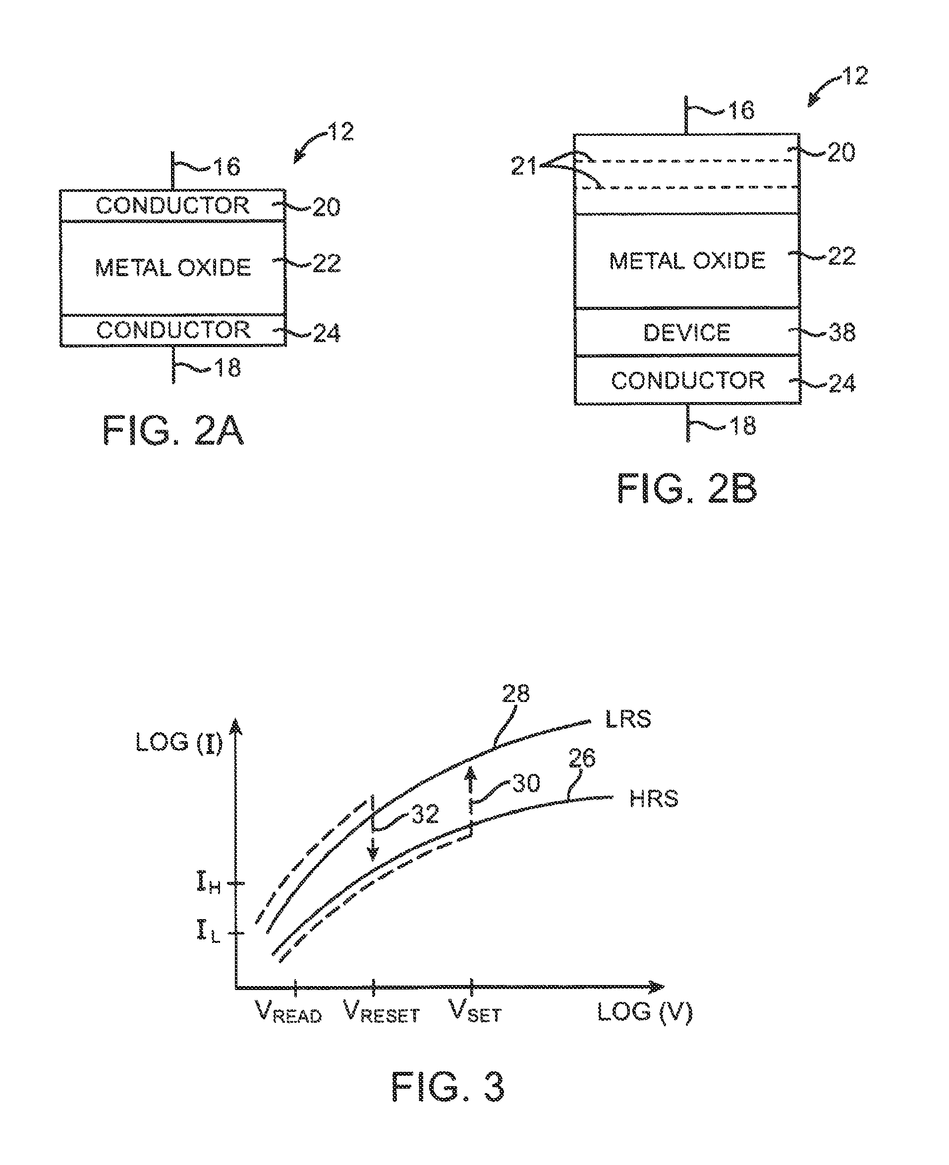
Embodiments of the invention include nonvolatile memory elements and memory devices comprising the nonvolatile memory elements. Methods for forming the nonvolatile memory elements are also disclosed. The nonvolatile memory element comprises a first electrode layer, a second electrode layer, and a plurality of layers of an oxide disposed between the first and second electrode layers. One of the oxide layers has linear resistance and substoichiometric composition, and the other oxide layer has bistable resistance and near-stoichiometric composition. Preferably, the sum of the two oxide layer thicknesses is between about 20 Å and about 100 Å, and the oxide layer with bistable resistance has a thickness between about 25% and about 75% of the total thickness. In one embodiment, the oxide layers are formed using reactive sputtering in an atmosphere with controlled flows of argon and oxygen.

Description

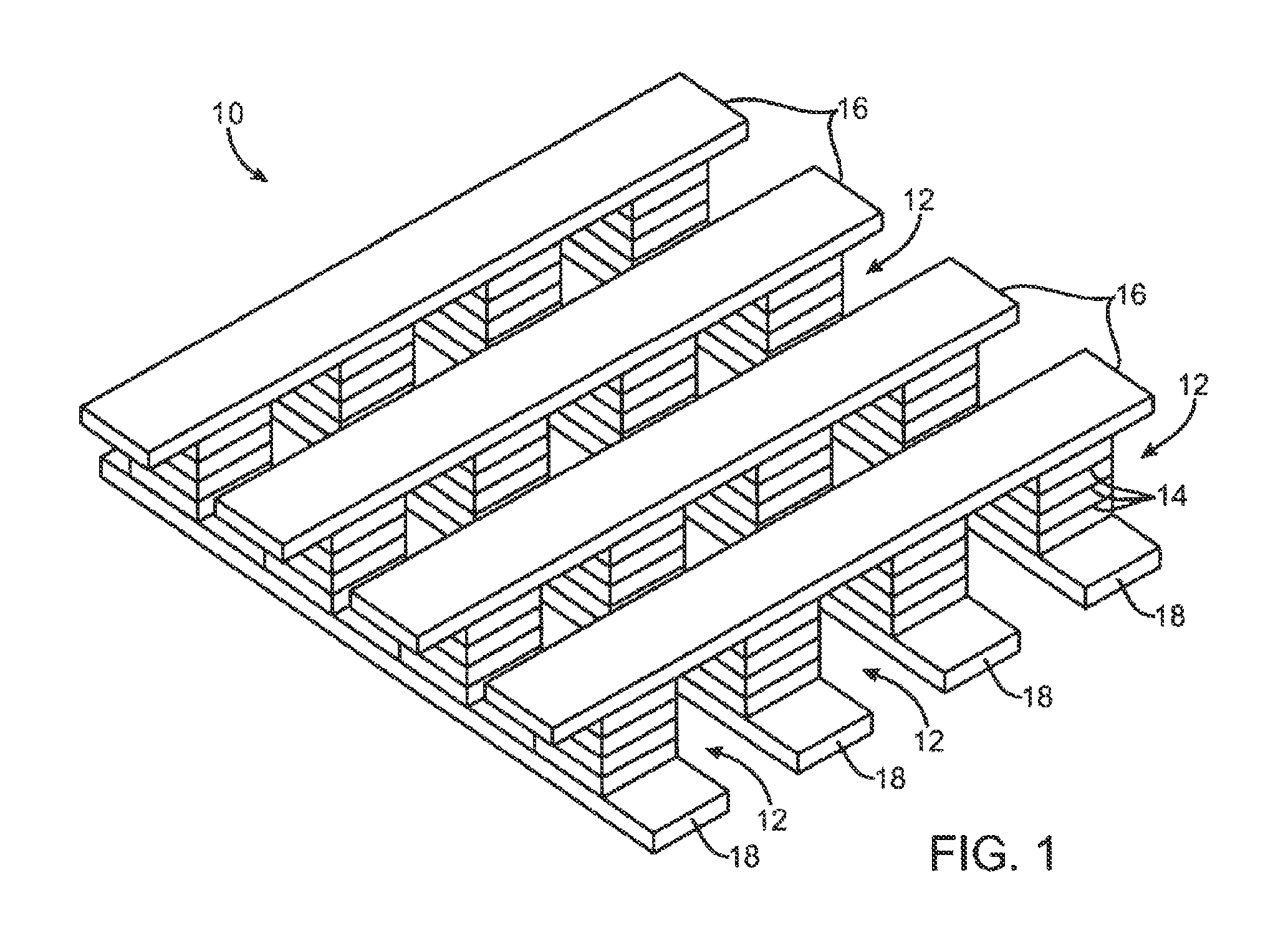
FIELD OF THE INVENTION[0001]One or more embodiments of the present invention relate to methods and apparatuses for depositing multiple layers of transition metal oxides of both stoichiometric and non-stoichiometric composition and any thickness.BACKGROUND[0002]Resistive random access memory (ReRAM) technologies are being proposed as a replacement for many semiconductor memory applications. These technologies can potentially enable the manufacture of non-volatile memories that are higher density, lower power, and faster access than technologies now in use.[0003]ReRAM comprises arrays of non-volatile memory elements each of which in turn comprise a volume of material that exhibits bistable resistance. The resistance state can be repeatedly switched back and forth between high and low values using modest write / erase voltages and power levels, and the resistance state can be read with lower voltage levels that do not change the state. Bistable resistance is typically created in a layer ...

Claims


Application Information

Patent Timeline
Patent Type & Authority Patents(United States)
IPC IPC(8): H01L29/02
CPCH01L45/1253H01L45/16H01L45/08H01L45/1233H01L45/146H01L45/1625H01L45/1641H01L45/145H01L27/2463H01L27/2409H10B63/20H10B63/80H10N70/24H10N70/826H10N70/8833H10N70/883H10N70/023H10N70/041H10N70/026H10N70/011H10N70/841H10N70/8836
Inventor PHAM, HIEUGOPAL, VIDYUTHASHIM, IMRANMINVIELLE, TIMWANG, YUNYAMAGUCHI, TAKESHIYANG, HONG SHENG
Owner SANDISK TECH LLC
Why Eureka
Try Eureka